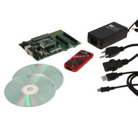
DV164136 Microchip Technology, DV164136 Datasheet - Page 278

DV164136
Manufacturer Part Number
DV164136
Description
DEVELOPMENT KIT FOR PIC18
Manufacturer
Microchip Technology
Series
PIC®r
Type
MCUr
Datasheets
1.DM183032.pdf
(38 pages)
2.DV164136.pdf
(448 pages)
3.DV164136.pdf
(6 pages)
4.DV164136.pdf
(446 pages)
5.DV164136.pdf
(4 pages)
6.DV164136.pdf
(18 pages)
Specifications of DV164136
Contents
Board, Cables, CDs, PICkit™ 3 Programmer, Power Supply
Processor To Be Evaluated
PIC18F8722, PIC18F87J11
Interface Type
RS-232, USB
Operating Supply Voltage
3.3 V, 5 V
Silicon Manufacturer
Microchip
Core Architecture
PIC
Core Sub-architecture
PIC18
Silicon Core Number
PIC18F
Silicon Family Name
PIC18F8xxx
Kit Contents
PIC18 Exp Brd PICkit 3 Cable CD PSU
Lead Free Status / RoHS Status
Lead free / RoHS Compliant
For Use With/related Products
PIC18F8722, PIC18F87J11
Lead Free Status / Rohs Status
Lead free / RoHS Compliant
Available stocks
Company
Part Number
Manufacturer
Quantity
Price
Company:
Part Number:
DV164136
Manufacturer:
MICROCHIP
Quantity:
12 000
- DM183032 PDF datasheet
- DV164136 PDF datasheet #2
- DV164136 PDF datasheet #3
- DV164136 PDF datasheet #4
- DV164136 PDF datasheet #5
- DV164136 PDF datasheet #6
- Current page: 278 of 446
- Download datasheet (7Mb)
PIC18F8722 FAMILY
21.1
For the A/D converter to meet its specified accuracy,
the charge holding capacitor (C
to fully charge to the input channel voltage level. The
analog input model is shown in Figure 21-3. The
source impedance (R
switch (R
required to charge the capacitor C
switch (R
(V
at the analog input (due to pin leakage current). The
maximum recommended impedance for analog
sources is 2.5 kΩ. After the analog input channel is
selected (changed), the channel must be sampled for
at least the minimum acquisition time before starting a
conversion.
EQUATION 21-1:
EQUATION 21-2:
EQUATION 21-3:
DS39646C-page 276
T
V
or
T
T
T
T
Temperature coefficient is only required for temperatures > 25°C. Below 25°C, T
T
T
ACQ
DD
Note:
C
ACQ
AMP
COFF
C
ACQ
HOLD
). The source impedance affects the offset voltage
=
=
A/D Acquisition Requirements
SS
=
=
=
=
=
SS
=
=
) impedance varies over the device voltage
When the conversion is started, the
holding capacitor is disconnected from the
input pin.
Amplifier Settling Time + Holding Capacitor Charging Time + Temperature Coefficient
T
) impedance directly affect the time
AMP
T
0.2 μs
(Temp – 25°C)(0.02 μs/°C)
(85°C – 25°C)(0.02 μs/°C)
1.2 μs
-(C
-(25 pF) (1 kΩ + 2 kΩ + 2.5 kΩ) ln(0.0004883) μs
1.05 μs
0.2 μs + 1 μs + 1.2 μs
2.4 μs
(V
-(C
AMP
HOLD
+ T
REF
HOLD
+ T
C
– (V
ACQUISITION TIME
A/D MINIMUM CHARGING TIME
CALCULATING THE MINIMUM REQUIRED ACQUISITION TIME
S
+ T
)(R
C
) and the internal sampling
)(R
+ T
REF
COFF
IC
IC
+ R
COFF
/2048)) • (1 – e
+ R
HOLD
SS
SS
HOLD
+ R
+ R
) must be allowed
S
S
) ln(1/2047) μs
. The sampling
) ln(1/2048)
(-T
C
/C
HOLD
(R
IC
+ R
SS
+ R
S
To
Equation 21-1 may be used. This equation assumes
that 1/2 LSb error is used (1024 steps for the A/D). The
1/2 LSb error is the maximum error allowed for the A/D
to meet its specified resolution.
Example 21-3 shows the calculation of the minimum
required acquisition time T
based
assumptions:
C
Rs
Conversion Error
V
Temperature
))
HOLD
DD
)
calculate
on
COFF
the
= 0 ms.
the
=
=
≤
=
=
following
minimum
© 2008 Microchip Technology Inc.
25 pF
2.5 kΩ
1/2 LSb
5V → Rss = 2 kΩ
85°C (system max.)
ACQ
. This calculation is
application
acquisition
system
time,
Related parts for DV164136
Image
Part Number
Description
Manufacturer
Datasheet
Request
R

Part Number:
Description:
Manufacturer:
Microchip Technology Inc.
Datasheet:

Part Number:
Description:
Manufacturer:
Microchip Technology Inc.
Datasheet:

Part Number:
Description:
Manufacturer:
Microchip Technology Inc.
Datasheet:

Part Number:
Description:
Manufacturer:
Microchip Technology Inc.
Datasheet:

Part Number:
Description:
Manufacturer:
Microchip Technology Inc.
Datasheet:

Part Number:
Description:
Manufacturer:
Microchip Technology Inc.
Datasheet:

Part Number:
Description:
Manufacturer:
Microchip Technology Inc.
Datasheet:

Part Number:
Description:
Manufacturer:
Microchip Technology Inc.
Datasheet:


