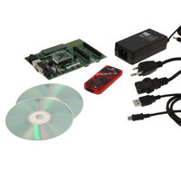
DV164136 Microchip Technology, DV164136 Datasheet - Page 209

DV164136
Manufacturer Part Number
DV164136
Description
DEVELOPMENT KIT FOR PIC18
Manufacturer
Microchip Technology
Series
PIC®r
Type
MCUr
Datasheets
1.DM183032.pdf
(38 pages)
2.DV164136.pdf
(448 pages)
3.DV164136.pdf
(6 pages)
4.DV164136.pdf
(446 pages)
5.DV164136.pdf
(4 pages)
6.DV164136.pdf
(18 pages)
Specifications of DV164136
Contents
Board, Cables, CDs, PICkit™ 3 Programmer, Power Supply
Processor To Be Evaluated
PIC18F8722, PIC18F87J11
Interface Type
RS-232, USB
Operating Supply Voltage
3.3 V, 5 V
Silicon Manufacturer
Microchip
Core Architecture
PIC
Core Sub-architecture
PIC18
Silicon Core Number
PIC18F
Silicon Family Name
PIC18F8xxx
Kit Contents
PIC18 Exp Brd PICkit 3 Cable CD PSU
Lead Free Status / RoHS Status
Lead free / RoHS Compliant
For Use With/related Products
PIC18F8722, PIC18F87J11
Lead Free Status / Rohs Status
Lead free / RoHS Compliant
Available stocks
Company
Part Number
Manufacturer
Quantity
Price
Company:
Part Number:
DV164136
Manufacturer:
MICROCHIP
Quantity:
12 000
- DM183032 PDF datasheet
- DV164136 PDF datasheet #2
- DV164136 PDF datasheet #3
- DV164136 PDF datasheet #4
- DV164136 PDF datasheet #5
- DV164136 PDF datasheet #6
- Current page: 209 of 446
- Download datasheet (7Mb)
REGISTER 19-2:
© 2008 Microchip Technology Inc.
bit 7
Legend:
R = Readable bit
-n = Value at POR
bit 7
bit 6
bit 5
bit 4
bit 3-0
Note 1:
WCOL
R/W-0
2:
3:
In Master mode, the overflow bit is not set since each new reception (and transmission) is initiated by
writing to the SSPxBUF register.
When enabled, these pins must be properly configured as input or output.
Bit combinations not specifically listed here are either reserved or implemented in I
WCOL: Write Collision Detect bit
1 = The SSPxBUF register is written while it is still transmitting the previous word
0 = No collision
SSPOV: Receive Overflow Indicator bit
SPI Slave mode:
1 = A new byte is received while the SSPxBUF register is still holding the previous data. In case of
0 = No overflow
SSPEN: Synchronous Serial Port Enable bit
1 = Enables serial port and configures SCKx, SDOx, SDIx and SSx as serial port pins
0 = Disables serial port and configures these pins as I/O port pins
CKP: Clock Polarity Select bit
1 = Idle state for clock is a high level
0 = Idle state for clock is a low level
SSPM<3:0>: Synchronous Serial Port Mode Select bits
0101 = SPI Slave mode, clock = SCKx pin, SSx pin control disabled, SSx can be used as I/O pin
0100 = SPI Slave mode, clock = SCKx pin, SSx pin control enabled
0011 = SPI Master mode, clock = TMR2 output/2
0010 = SPI Master mode, clock = F
0001 = SPI Master mode, clock = F
0000 = SPI Master mode, clock = F
SSPOV
R/W-0
(must be cleared in software)
overflow, the data in SSPxSR is lost. Overflow can only occur in Slave mode. The user must read
the SSPxBUF, even if only transmitting data, to avoid setting overflow (must be cleared in soft-
ware).
SSPxCON1: MSSPx CONTROL REGISTER 1 (SPI MODE)
(1)
W = Writable bit
‘1’ = Bit is set
SSPEN
R/W-0
(2)
R/W-0
CKP
OSC
OSC
OSC
(1)
/64
/16
/4
U = Unimplemented bit, read as ‘0’
‘0’ = Bit is cleared
(2)
SSPM3
R/W-0
PIC18F8722 FAMILY
(3)
(3)
SSPM2
R/W-0
(3)
x = Bit is unknown
SSPM1
R/W-0
2
C™ mode only.
(3)
DS39646C-page 207
SSPM0
R/W-0
bit 0
(3)
Related parts for DV164136
Image
Part Number
Description
Manufacturer
Datasheet
Request
R

Part Number:
Description:
Manufacturer:
Microchip Technology Inc.
Datasheet:

Part Number:
Description:
Manufacturer:
Microchip Technology Inc.
Datasheet:

Part Number:
Description:
Manufacturer:
Microchip Technology Inc.
Datasheet:

Part Number:
Description:
Manufacturer:
Microchip Technology Inc.
Datasheet:

Part Number:
Description:
Manufacturer:
Microchip Technology Inc.
Datasheet:

Part Number:
Description:
Manufacturer:
Microchip Technology Inc.
Datasheet:

Part Number:
Description:
Manufacturer:
Microchip Technology Inc.
Datasheet:

Part Number:
Description:
Manufacturer:
Microchip Technology Inc.
Datasheet:


