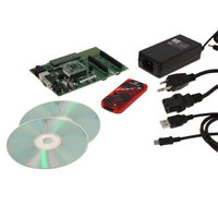
DV164136 Microchip Technology, DV164136 Datasheet - Page 113

DV164136
Manufacturer Part Number
DV164136
Description
DEVELOPMENT KIT FOR PIC18
Manufacturer
Microchip Technology
Series
PIC®r
Type
MCUr
Datasheets
1.DM183032.pdf
(38 pages)
2.DV164136.pdf
(448 pages)
3.DV164136.pdf
(6 pages)
4.DV164136.pdf
(446 pages)
5.DV164136.pdf
(4 pages)
6.DV164136.pdf
(18 pages)
Specifications of DV164136
Contents
Board, Cables, CDs, PICkit™ 3 Programmer, Power Supply
Processor To Be Evaluated
PIC18F8722, PIC18F87J11
Interface Type
RS-232, USB
Operating Supply Voltage
3.3 V, 5 V
Silicon Manufacturer
Microchip
Core Architecture
PIC
Core Sub-architecture
PIC18
Silicon Core Number
PIC18F
Silicon Family Name
PIC18F8xxx
Kit Contents
PIC18 Exp Brd PICkit 3 Cable CD PSU
Lead Free Status / RoHS Status
Lead free / RoHS Compliant
For Use With/related Products
PIC18F8722, PIC18F87J11
Lead Free Status / Rohs Status
Lead free / RoHS Compliant
Available stocks
Company
Part Number
Manufacturer
Quantity
Price
Company:
Part Number:
DV164136
Manufacturer:
MICROCHIP
Quantity:
12 000
- DM183032 PDF datasheet
- DV164136 PDF datasheet #2
- DV164136 PDF datasheet #3
- DV164136 PDF datasheet #4
- DV164136 PDF datasheet #5
- DV164136 PDF datasheet #6
- Current page: 113 of 446
- Download datasheet (7Mb)
8.0
The data EEPROM is a nonvolatile memory array,
separate from the data RAM and program memory, that
is used for long-term storage of program data. It is not
directly mapped in either the register file or program
memory space, but is indirectly addressed through the
Special Function Registers (SFRs). The EEPROM is
readable and writable during normal operation over the
entire V
Five SFRs are used to read and write to the data
EEPROM, as well as the program memory. They are:
• EECON1
• EECON2
• EEDATA
• EEADR
• EEADRH
The data EEPROM allows byte read and write. When
interfacing to the data memory block, EEDATA holds
the 8-bit data for read/write and the EEADRH:EEADR
register pair holds the address of the EEPROM location
being accessed.
The EEPROM data memory is rated for high erase/write
cycle endurance. A byte write automatically erases the
location and writes the new data (erase-before-write).
The write time is controlled by an on-chip timer; it will
vary with voltage and temperature, as well as from chip-
to-chip. Please refer to parameter D122 (Table 28-1 in
Section 28.0 “Electrical Characteristics”) for exact
limits.
8.1
The EEADRH:EEADR register pair is used to address
the data EEPROM for read and write operations.
EEADRH holds the two MSbs of the address; the upper
6 bits are ignored. The 10-bit range of the pair can
address a memory range of 1024 bytes (00h to 3FFh).
© 2008 Microchip Technology Inc.
DD
DATA EEPROM MEMORY
EEADR and EEADRH Registers
range.
8.2
Access to the data EEPROM is controlled by two
registers: EECON1 and EECON2. These are the same
registers which control access to the program memory
and are used in a similar manner for the data
EEPROM.
The EECON1 register (Register ) is the control register
for data and program memory access. Control bit
EEPGD determines if the access will be to program or
data EEPROM memory. When clear, operations will
access the data EEPROM memory. When set, program
memory is accessed.
Control bit CFGS determines if the access will be to the
Configuration registers or to program memory/data
EEPROM memory. When set, subsequent operations
access Configuration registers. When CFGS is clear,
the EEPGD bit selects either program Flash or data
EEPROM memory.
The WREN bit, when set, will allow a write operation.
On power-up, the WREN bit is clear. The WRERR bit is
set in hardware when the WREN bit is set and cleared
when the internal programming timer expires and the
write operation is complete.
The WR control bit initiates write operations. The bit
cannot be cleared, only set, in software; it is cleared in
hardware at the completion of the write operation.
Control bits, RD and WR, start read and erase/write
operations, respectively. These bits are set by firmware
and cleared by hardware at the completion of the
operation.
The RD bit cannot be set when accessing program
memory (EEPGD = 1). Program memory is read using
table read instructions. See Section 6.1 “Table Reads
and Table Writes” regarding table reads.
The EECON2 register is not a physical register. It is
used exclusively in the memory write and erase
sequences. Reading EECON2 will read all ‘0’s.
PIC18F8722 FAMILY
Note:
Note:
EECON1 and EECON2 Registers
During normal operation, the WRERR is
read as ‘1’. This can indicate that a write
operation was prematurely terminated by
a Reset, or a write operation was
attempted improperly.
The EEIF interrupt flag bit (PIR2<4>) is set
when the write is complete. It must be
cleared in software.
DS39646C-page 111
Related parts for DV164136
Image
Part Number
Description
Manufacturer
Datasheet
Request
R

Part Number:
Description:
Manufacturer:
Microchip Technology Inc.
Datasheet:

Part Number:
Description:
Manufacturer:
Microchip Technology Inc.
Datasheet:

Part Number:
Description:
Manufacturer:
Microchip Technology Inc.
Datasheet:

Part Number:
Description:
Manufacturer:
Microchip Technology Inc.
Datasheet:

Part Number:
Description:
Manufacturer:
Microchip Technology Inc.
Datasheet:

Part Number:
Description:
Manufacturer:
Microchip Technology Inc.
Datasheet:

Part Number:
Description:
Manufacturer:
Microchip Technology Inc.
Datasheet:

Part Number:
Description:
Manufacturer:
Microchip Technology Inc.
Datasheet:


