DV164136 Microchip Technology, DV164136 Datasheet - Page 37

DV164136
Manufacturer Part Number
DV164136
Description
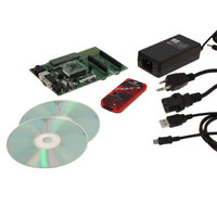
DEVELOPMENT KIT FOR PIC18
Manufacturer
Microchip Technology
Series
PIC®r
Type
MCUr
Datasheets
1.DM183032.pdf
(38 pages)
2.DV164136.pdf
(448 pages)
3.DV164136.pdf
(6 pages)
4.DV164136.pdf
(446 pages)
5.DV164136.pdf
(4 pages)
6.DV164136.pdf
(18 pages)
Specifications of DV164136
Contents
Board, Cables, CDs, PICkit™ 3 Programmer, Power Supply
Processor To Be Evaluated
PIC18F8722, PIC18F87J11
Interface Type
RS-232, USB
Operating Supply Voltage
3.3 V, 5 V
Silicon Manufacturer
Microchip
Core Architecture
PIC
Core Sub-architecture
PIC18
Silicon Core Number
PIC18F
Silicon Family Name
PIC18F8xxx
Kit Contents
PIC18 Exp Brd PICkit 3 Cable CD PSU
Lead Free Status / RoHS Status
Lead free / RoHS Compliant
For Use With/related Products
PIC18F8722, PIC18F87J11
Lead Free Status / Rohs Status
Lead free / RoHS Compliant
Available stocks
Company
Part Number
Manufacturer
Quantity
Price
Company:
Part Number:
DV164136
Manufacturer:
MICROCHIP
Quantity:
12 000
- DM183032 PDF datasheet
- DV164136 PDF datasheet #2
- DV164136 PDF datasheet #3
- DV164136 PDF datasheet #4
- DV164136 PDF datasheet #5
- DV164136 PDF datasheet #6
- Current page: 37 of 446
- Download datasheet (7Mb)
2.6.4
The 4x Phase Locked Loop (PLL) can be used with the
internal oscillator block to produce faster device clock
speeds than are normally possible with the internal
oscillator sources. When enabled, the PLL produces a
clock speed of 16 MHz or 32 MHz.
Unlike HSPLL mode, the PLL is controlled through
software. The control bit, PLLEN (OSCTUNE<6>), is
used to enable or disable its operation.
The PLL is available when the device is configured to
use the internal oscillator block as its primary clock
source (FOSC<3:0> = 1001 or 1000). Additionally, the
PLL will only function when the selected output fre-
quency is either 4 MHz or 8 MHz (OSCCON<6:4> = 111
or 110). If both of these conditions are not met, the PLL
is disabled and the PLLEN bit remains clear (writes are
ignored).
REGISTER 2-1:
© 2008 Microchip Technology Inc.
bit 7
Legend:
R = Readable bit
-n = Value at POR
bit 7
bit 6
bit 5
bit 4-0
Note 1:
INTSRC
R/W-0
Available only in certain oscillator configurations; otherwise, this bit is unavailable and reads as ‘0’. See
Section 2.6.4 “PLL in INTOSC Modes” for details.
PLL IN INTOSC MODES
INTSRC: Internal Oscillator Low-Frequency Source Select bit
1 = 31.25 kHz device clock derived from 8 MHz INTOSC source (divide-by-256 enabled)
0 = 31 kHz device clock derived directly from INTRC internal oscillator
PLLEN: Frequency Multiplier PLL for INTOSC Enable bit
1 = PLL enabled for INTOSC (4 MHz and 8 MHz only)
0 = PLL disabled
Unimplemented: Read as ‘0’
TUN<4:0>: Frequency Tuning bits
01111 = Maximum frequency
•
•
00001
00000 = Center frequency. Oscillator module is running at the calibrated frequency.
11111
•
•
10000 = Minimum frequency
PLLEN
R/W-0
OSCTUNE: OSCILLATOR TUNING REGISTER
(1)
W = Writable bit
‘1’ = Bit is set
•
•
•
•
U-0
—
R/W-0
TUN4
U = Unimplemented bit, read as ‘0’
‘0’ = Bit is cleared
R/W-0
TUN3
2.6.5
The factory calibrates the internal oscillator block
output (INTOSC) for 8 MHz. However, this frequency
may drift as V
affect the controller operation in a variety of ways. It is
possible to adjust the INTOSC frequency by modifying
the value in the OSCTUNE register. Depending on the
device, this may have no effect on the INTRC clock
source frequency.
Tuning the INTOSC source requires knowing when to
make the adjustment, in which direction it should be
made and in some cases, how large a change is
needed. Three compensation techniques are discussed
in
EUSART”, Section 2.6.5.2 “Compensating with the
Timers” and Section 2.6.5.3 “Compensating with the
CCP Module in Capture Mode” but other techniques
may be used.
PIC18F8722 FAMILY
Section 2.6.5.1
(1)
INTOSC FREQUENCY DRIFT
R/W-0
TUN2
DD
or temperature changes and can
“Compensating
x = Bit is unknown
R/W-0
TUN1
DS39646C-page 35
with
R/W-0
TUN0
bit 0
the
Related parts for DV164136
Image
Part Number
Description
Manufacturer
Datasheet
Request
R

Part Number:
Description:
Manufacturer:
Microchip Technology Inc.
Datasheet:

Part Number:
Description:
Manufacturer:
Microchip Technology Inc.
Datasheet:

Part Number:
Description:
Manufacturer:
Microchip Technology Inc.
Datasheet:

Part Number:
Description:
Manufacturer:
Microchip Technology Inc.
Datasheet:

Part Number:
Description:
Manufacturer:
Microchip Technology Inc.
Datasheet:

Part Number:
Description:
Manufacturer:
Microchip Technology Inc.
Datasheet:

Part Number:
Description:
Manufacturer:
Microchip Technology Inc.
Datasheet:

Part Number:
Description:
Manufacturer:
Microchip Technology Inc.
Datasheet:


