Z8F64220100ZDA Zilog, Z8F64220100ZDA Datasheet - Page 28
Z8F64220100ZDA
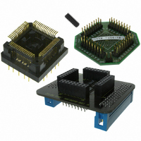
Manufacturer Part Number
Z8F64220100ZDA
Description
ADAPTER ICE Z8 ENCORE 64K 64LQFP
Manufacturer
Zilog
Specifications of Z8F64220100ZDA
Module/board Type
*
For Use With/related Products
Z8 Encore!™
Lead Free Status / RoHS Status
Contains lead / RoHS non-compliant
Other names
269-3403


Table 3. Signal Descriptions (Continued)
PS019921-0308
Signal
Mnemonic
SCK
MOSI
MISO
UART Controllers
TXD0 / TXD1
RXD0 / RXD1
CTS0
DE0 / DE1
Timers
T0OUT/T1OUT/
T2OUT/T3OUT
T0IN/T1IN/
T2IN/T3IN
Analog
ANA[11:0]
VREF
Oscillators
/
CTS1
I/O
I/O
I/O
I/O
O
I
I
O
O
I
I
I
Description
SPI Serial Clock. The SPI master supplies this pin. If the Z8 Encore! XP
F64XX Series is the SPI master, this pin is an output. If the Z8 Encore! XP
F64XX Series is the SPI slave, this pin is an input. It is multiplexed with a
general-purpose I/O pin.
Master-Out/Slave-In. This signal is the data output from the SPI master
device and the data input to the SPI slave device. It is multiplexed with a
general-purpose I/O pin.
Master-In/Slave-Out. This pin is the data input to the SPI master device and
the data output from the SPI slave device. It is multiplexed with a
general-purpose I/O pin.
Transmit Data. These signals are the transmit outputs from the UARTs. The
TXD signals are multiplexed with general-purpose I/O pins.
Receive Data. These signals are the receiver inputs for the UARTs and
IrDAs. The RXD signals are multiplexed with general-purpose I/O pins.
Clear To Send. These signals are control inputs for the UARTs. The CTS
signals are multiplexed with general-purpose I/O pins.
Driver Enable. This signal allows automatic control of external RS-485
drivers. This signal is approximately the inverse of the Transmit Empty (TXE)
bit in the UART Status 0 register. The DE signal may be used to ensure an
external RS-485 driver is enabled when data is transmitted by the UART.
Timer Output 0-3. These signals are output pins from the timers. The Timer
Output signals are multiplexed with general-purpose I/O pins. T3OUT is not
available in 44-pin package devices.
Timer Input 0-3. These signals are used as the capture, gating and counter
inputs. The Timer Input signals are multiplexed with general-purpose I/O
pins. T3IN is not available in 44-pin package devices.
Analog Input. These signals are inputs to the ADC. The ADC analog inputs
are multiplexed with general-purpose I/O pins.
Analog-to-Digital converter reference voltage input. The VREF pin must be
left unconnected (or capacitively coupled to analog ground) if the internal
voltage reference is selected as the ADC reference voltage.
Z8 Encore! XP
Product Specification
Signal and Pin Descriptions
®
F64XX Series
14
Related parts for Z8F64220100ZDA
Image
Part Number
Description
Manufacturer
Datasheet
Request
R

Part Number:
Description:
Communication Controllers, ZILOG INTELLIGENT PERIPHERAL CONTROLLER (ZIP)
Manufacturer:
Zilog, Inc.
Datasheet:

Part Number:
Description:
KIT DEV FOR Z8 ENCORE 16K TO 64K
Manufacturer:
Zilog
Datasheet:

Part Number:
Description:
KIT DEV Z8 ENCORE XP 28-PIN
Manufacturer:
Zilog
Datasheet:

Part Number:
Description:
DEV KIT FOR Z8 ENCORE 8K/4K
Manufacturer:
Zilog
Datasheet:

Part Number:
Description:
KIT DEV Z8 ENCORE XP 28-PIN
Manufacturer:
Zilog
Datasheet:

Part Number:
Description:
DEV KIT FOR Z8 ENCORE 4K TO 8K
Manufacturer:
Zilog
Datasheet:
Part Number:
Description:
CMOS Z8 microcontroller. ROM 16 Kbytes, RAM 256 bytes, speed 16 MHz, 32 lines I/O, 3.0V to 5.5V
Manufacturer:
Zilog, Inc.
Datasheet:
Part Number:
Description:
Low-cost microcontroller. 512 bytes ROM, 61 bytes RAM, 8 MHz
Manufacturer:
Zilog, Inc.
Datasheet:
Part Number:
Description:
Z8 4K OTP Microcontroller
Manufacturer:
Zilog, Inc.
Datasheet:
Part Number:
Description:
CMOS SUPER8 ROMLESS MCU
Manufacturer:
Zilog, Inc.
Datasheet:
Part Number:
Description:
SL1866 CMOSZ8 OTP Microcontroller
Manufacturer:
Zilog, Inc.
Datasheet:
Part Number:
Description:
SL1866 CMOSZ8 OTP Microcontroller
Manufacturer:
Zilog, Inc.
Datasheet:
Part Number:
Description:
OTP (KB) = 1, RAM = 125, Speed = 12, I/O = 14, 8-bit Timers = 2, Comm Interfaces Other Features = Por, LV Protect, Voltage = 4.5-5.5V
Manufacturer:
Zilog, Inc.
Datasheet:
Part Number:
Description:
Manufacturer:
Zilog, Inc.
Datasheet: