APMOTOR56F8000E Freescale Semiconductor, APMOTOR56F8000E Datasheet - Page 70
APMOTOR56F8000E
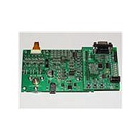
Manufacturer Part Number
APMOTOR56F8000E
Description
KIT DEMO MOTOR CTRL SYSTEM
Manufacturer
Freescale Semiconductor
Type
Motor / Motion Controllers & Driversr
Datasheets
1.CWH-UTP-ONCE-HE.pdf
(2 pages)
2.APMOTOR56F8000E.pdf
(124 pages)
3.APMOTOR56F8000E.pdf
(2 pages)
Specifications of APMOTOR56F8000E
Accessory Type
Motor Controller
Input Voltage
9 V
Interface Type
RS-232
Product
Power Management Modules
For Use With/related Products
DEMO56F8013, DEMO56F8013-E
Lead Free Status / RoHS Status
Lead free / RoHS Compliant


The lower four bits of the GPIO A register can function as GPIO, PWM, or as additional clock output
signals. GPIO has priority and is enabled/disabled via the GPIOA_PEREN. If GPIOA[3:0] are
programmed to operate as peripheral outputs, then the choice between PWM and additional clock outputs
is done here in the CLKOUT. The default state is for the peripheral function of GPIOA[3:0] to be
programmed as PWM. This can be changed by altering PWM3 through PWM0.
6.3.7.1
This bit field is reserved or not implemented. It is read as 0 and cannot be modified by writing.
6.3.7.2
6.3.7.3
6.3.7.4
6.3.7.5
6.3.7.6
6.3.7.7
Selects clock to be muxed out on the CLKO pin.
70
•
•
•
•
•
•
•
•
•
•
•
•
•
•
Base + $A
RESET
0 = Peripheral output function of GPIOA[3] is defined to be PWM3
1 = Peripheral output function of GPIOA[3] is defined to be the Relaxation Oscillator Clock
0 = Peripheral output function of GPIOA[2] is defined to be PWM2
1 = Peripheral output function of GPIOA[2] is defined to be the system clock
0 = Peripheral output function of GPIOA[1] is defined to be PWM1
1 = Peripheral output function of GPIOA[1] is defined to be two times the rate of the system clock
0 = Peripheral output function of GPIOA[0] is defined to be PWM0
1 = Peripheral output function of GPIOA[0] is defined to be three times the rate of the system clock
0 = CLKOUT output is enabled and will output the signal indicated by CLKOSEL
1 = CLKOUT is 0
00000 = Reserved for factory test—Continuous system clock
01001 = Reserved for factory test—OCCS MSTR OSC clock
01011 = Reserved for factory test—ADC clock
01100 = Reserved for factory test—JTAG TCLK
Read
Write
Reserved—Bits 15–10
PWM3—Bit 9
PWM2—Bit 8
PWM1—Bit 7
PWM0—Bit 6
Clockout Disable (CLKDIS)—Bit 5
Clockout Select (CLKOSEL)—Bits 4–0
15
0
0
14
0
0
Figure 6-8 CLKO Select Register (SIM_CLKOUT)
13
0
0
12
0
0
56F8014 Technical Data, Rev. 11
11
0
0
10
0
0
PWM
9
3
0
PWM
8
2
0
PWM1 PWM0
7
0
6
0
CLK
DIS
5
1
4
0
3
0
Freescale Semiconductor
CLKOSEL
2
0
1
0
0
0
Related parts for APMOTOR56F8000E
Image
Part Number
Description
Manufacturer
Datasheet
Request
R

Part Number:
Description:
Manufacturer:
Freescale Semiconductor, Inc
Datasheet:
Part Number:
Description:
Manufacturer:
Freescale Semiconductor, Inc
Datasheet:
Part Number:
Description:
Manufacturer:
Freescale Semiconductor, Inc
Datasheet:
Part Number:
Description:
Manufacturer:
Freescale Semiconductor, Inc
Datasheet:
Part Number:
Description:
Manufacturer:
Freescale Semiconductor, Inc
Datasheet:
Part Number:
Description:
Manufacturer:
Freescale Semiconductor, Inc
Datasheet:
Part Number:
Description:
Manufacturer:
Freescale Semiconductor, Inc
Datasheet:
Part Number:
Description:
Manufacturer:
Freescale Semiconductor, Inc
Datasheet:
Part Number:
Description:
Manufacturer:
Freescale Semiconductor, Inc
Datasheet:
Part Number:
Description:
Manufacturer:
Freescale Semiconductor, Inc
Datasheet:
Part Number:
Description:
Manufacturer:
Freescale Semiconductor, Inc
Datasheet:
Part Number:
Description:
Manufacturer:
Freescale Semiconductor, Inc
Datasheet:
Part Number:
Description:
Manufacturer:
Freescale Semiconductor, Inc
Datasheet:
Part Number:
Description:
Manufacturer:
Freescale Semiconductor, Inc
Datasheet:
Part Number:
Description:
Manufacturer:
Freescale Semiconductor, Inc
Datasheet: