APMOTOR56F8000E Freescale Semiconductor, APMOTOR56F8000E Datasheet - Page 22
APMOTOR56F8000E
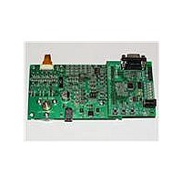
Manufacturer Part Number
APMOTOR56F8000E
Description
KIT DEMO MOTOR CTRL SYSTEM
Manufacturer
Freescale Semiconductor
Type
Motor / Motion Controllers & Driversr
Datasheets
1.CWH-UTP-ONCE-HE.pdf
(2 pages)
2.APMOTOR56F8000E.pdf
(124 pages)
3.APMOTOR56F8000E.pdf
(2 pages)
Specifications of APMOTOR56F8000E
Accessory Type
Motor Controller
Input Voltage
9 V
Interface Type
RS-232
Product
Power Management Modules
For Use With/related Products
DEMO56F8013, DEMO56F8013-E
Lead Free Status / RoHS Status
Lead free / RoHS Compliant


22
Table 2-3 56F8014 Signal and Package Information for the 32-Pin LQFP (Continued)
5. This signal is also brought out on the GPIOA4 pin.
6. This signal is also brought out on the GPIOA5 pin.
Return to
GPIOB2
GPIOB3
GPIOA0
(PWM0)
(MISO)
(MOSI)
Signal
Name
(T2
(T3
5
6
)
)
Table 2-2
Pin No.
LQFP
18
17
28
Output
Output
Output
Output
Output
Output
Output
Output
Input/
Input/
Input/
Input/
Input/
Input/
Input/
Type
State During
Input with
Input with
Input with
enabled
enabled
enabled
internal
internal
internal
pull-up
pull-up
pull-up
Reset
56F8014 Technical Data, Rev. 11
Port B GPIO — This GPIO pin can be individually programmed as
an input or output pin.
SPI Master In/Slave Out — This serial data pin is an input to a
master device and an output from a slave device. The MISO line of a
slave device is placed in the high-impedance state if the slave device
is not selected. The slave device places data on the MISO line a
half-cycle before the clock edge the master device uses to latch the
data.
T2 — Timer, Channel 2
After reset, the default state is GPIOB2. The alternative peripheral
functionality is controlled via the SIM. See
Port B GPIO — This GPIO pin can be individually programmed as
an input or output pin.
SPI Master Out/Slave In— This serial data pin is an output from a
master device and an input to a slave device. The master device
places data on the MOSI line a half-cycle before the clock edge the
slave device uses to latch the data.
T3 — Timer, Channel 3
After reset, the default state is GPIOB3. The alternative peripheral
functionality is controlled via the SIM. See
Port A GPIO — This GPIO pin can be individually programmed as
an input or output pin.
PWM0 — This is one of the six PWM output pins.
After reset, the default state is GPIOA0.
Signal Description
Section
Section
Freescale Semiconductor
6.3.8.
6.3.8.
Related parts for APMOTOR56F8000E
Image
Part Number
Description
Manufacturer
Datasheet
Request
R

Part Number:
Description:
Manufacturer:
Freescale Semiconductor, Inc
Datasheet:
Part Number:
Description:
Manufacturer:
Freescale Semiconductor, Inc
Datasheet:
Part Number:
Description:
Manufacturer:
Freescale Semiconductor, Inc
Datasheet:
Part Number:
Description:
Manufacturer:
Freescale Semiconductor, Inc
Datasheet:
Part Number:
Description:
Manufacturer:
Freescale Semiconductor, Inc
Datasheet:
Part Number:
Description:
Manufacturer:
Freescale Semiconductor, Inc
Datasheet:
Part Number:
Description:
Manufacturer:
Freescale Semiconductor, Inc
Datasheet:
Part Number:
Description:
Manufacturer:
Freescale Semiconductor, Inc
Datasheet:
Part Number:
Description:
Manufacturer:
Freescale Semiconductor, Inc
Datasheet:
Part Number:
Description:
Manufacturer:
Freescale Semiconductor, Inc
Datasheet:
Part Number:
Description:
Manufacturer:
Freescale Semiconductor, Inc
Datasheet:
Part Number:
Description:
Manufacturer:
Freescale Semiconductor, Inc
Datasheet:
Part Number:
Description:
Manufacturer:
Freescale Semiconductor, Inc
Datasheet:
Part Number:
Description:
Manufacturer:
Freescale Semiconductor, Inc
Datasheet:
Part Number:
Description:
Manufacturer:
Freescale Semiconductor, Inc
Datasheet: