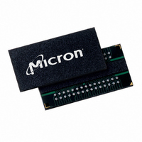
MT46H8M16LFCF-10 Micron Technology Inc, MT46H8M16LFCF-10 Datasheet - Page 54

MT46H8M16LFCF-10
Manufacturer Part Number
MT46H8M16LFCF-10
Description
IC DDR SDRAM 128MBIT 60VFBGA
Manufacturer
Micron Technology Inc
Type
DDR SDRAMr
Specifications of MT46H8M16LFCF-10
Format - Memory
RAM
Memory Type
Mobile DDR SDRAM
Memory Size
128M (8Mx16)
Speed
100MHz
Interface
Parallel
Voltage - Supply
1.7 V ~ 1.9 V
Operating Temperature
0°C ~ 70°C
Package / Case
60-VFBGA
Organization
8Mx16
Density
128Mb
Address Bus
15b
Access Time (max)
7ns
Maximum Clock Rate
104MHz
Operating Supply Voltage (typ)
1.8V
Package Type
VFBGA
Operating Temp Range
0C to 70C
Operating Supply Voltage (max)
1.9V
Operating Supply Voltage (min)
1.7V
Supply Current
90mA
Pin Count
60
Mounting
Surface Mount
Operating Temperature Classification
Commercial
Lead Free Status / RoHS Status
Lead free / RoHS Compliant
Available stocks
Company
Part Number
Manufacturer
Quantity
Price
Company:
Part Number:
MT46H8M16LFCF-10
Manufacturer:
Micron Technology Inc
Quantity:
10 000
Company:
Part Number:
MT46H8M16LFCF-10 IT
Manufacturer:
Micron Technology Inc
Quantity:
10 000
Company:
Part Number:
MT46H8M16LFCF-10 IT TR
Manufacturer:
Micron Technology Inc
Quantity:
10 000
Company:
Part Number:
MT46H8M16LFCF-10 TR
Manufacturer:
Micron Technology Inc
Quantity:
10 000
PDF: 09005aef822b7e27/Source: 09005aef822b7dd6
MT46H8M16LFB_2.fm - Rev. A 5/06 EN
33. V
34.
35. I
36. Random addressing changing 50 percent of data changing at every transfer.
37. Random addressing changing 100 percent of data changing at every transfer.
38. CKE must be active (HIGH) during the entire time a REFRESH command is executed.
39. With the inclusion of the temperature sensor on the low-power DDR device, these
40. The transition time for input signals (CAS#, CKE, CS#, DM, DQ, DQS, RAS#, WE#, and
41.
42. These parameters guarantee device timing but they are not necessarily tested on each
43. Clock must be toggled a minimum of two times during this period.
44. Clock must be toggled a minimum of one time during this period.
can not be greater than 1/3 of the cycle rate. V
pulse width ≤ 3ns and the pulse width can not be greater than 1/3 of the cycle rate.
t
I
remain stable. Although I
That is, from the time the AUTO REFRESH command is registered, CKE must be
active at each rising clock edge, until
numbers are shown as examples only, and will change due to the junction tempera-
ture that the device is sensing. They are expected to be maximum values at this time.
addresses) are measured between V
V
t
next higher integer.
device.
HZ (MAX) will prevail over
DAL = (
DD
DD
IH
IH
(
2N specifies DQ, DQS, and DM to be driven to a valid HIGH or LOW logic level.
2Q is similar to I
overshoot: V
DC
) to V
t
WR/
IL
t
(
CK) + (
AC
IH
) for falling input signals.
(MAX) = V
DD
t
RP/
2F except I
t
DD
CK): for each term, if not already an integer, round to the
54
t
DQSCK (MAX) +
2F, I
DD
Q + 0.5V for a pulse width ≤ 3ns and the pulse width
DD
DD
128Mb: 8 Meg x 16 Mobile DDR SDRAM
2N, and I
IL
2Q specifies the address and control inputs to
Micron Technology, Inc., reserves the right to change products or specifications without notice.
t
(
RFC later.
DC
) to V
DD
t
RPST (MAX) condition.
IL
IH
2Q are similar, I
undershoot: V
(
AC
) for rising input signals and
©2006 Micron Technology, Inc. All rights reserved.
DD
IL
(MIN) = –0.5V for a
2F is “worst case.”
Advance
Notes


