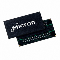
MT46H8M16LFCF-10 Micron Technology Inc, MT46H8M16LFCF-10 Datasheet - Page 19

MT46H8M16LFCF-10
Manufacturer Part Number
MT46H8M16LFCF-10
Description
IC DDR SDRAM 128MBIT 60VFBGA
Manufacturer
Micron Technology Inc
Type
DDR SDRAMr
Specifications of MT46H8M16LFCF-10
Format - Memory
RAM
Memory Type
Mobile DDR SDRAM
Memory Size
128M (8Mx16)
Speed
100MHz
Interface
Parallel
Voltage - Supply
1.7 V ~ 1.9 V
Operating Temperature
0°C ~ 70°C
Package / Case
60-VFBGA
Organization
8Mx16
Density
128Mb
Address Bus
15b
Access Time (max)
7ns
Maximum Clock Rate
104MHz
Operating Supply Voltage (typ)
1.8V
Package Type
VFBGA
Operating Temp Range
0C to 70C
Operating Supply Voltage (max)
1.9V
Operating Supply Voltage (min)
1.7V
Supply Current
90mA
Pin Count
60
Mounting
Surface Mount
Operating Temperature Classification
Commercial
Lead Free Status / RoHS Status
Lead free / RoHS Compliant
Available stocks
Company
Part Number
Manufacturer
Quantity
Price
Company:
Part Number:
MT46H8M16LFCF-10
Manufacturer:
Micron Technology Inc
Quantity:
10 000
Company:
Part Number:
MT46H8M16LFCF-10 IT
Manufacturer:
Micron Technology Inc
Quantity:
10 000
Company:
Part Number:
MT46H8M16LFCF-10 IT TR
Manufacturer:
Micron Technology Inc
Quantity:
10 000
Company:
Part Number:
MT46H8M16LFCF-10 TR
Manufacturer:
Micron Technology Inc
Quantity:
10 000
Operations
Bank/row Activation
Figure 7:
PDF: 09005aef822b7e27/Source: 09005aef822b7dd6
MT46H8M16LFB_2.fm - Rev. A 5/06 EN
Activating a Specific Row in a Specific Bank
Notes:
1. BA = Bank address
Before any READ or WRITE commands can be issued to a bank within the Mobile DDR
SDRAM, a row in that bank must be “opened.” This is accomplished via the ACTIVE
command, which selects both the bank and the row to be activated, as shown in
Figure 7.
After a row is opened with an ACTIVE command, a READ or WRITE command may be
issued to that row, subject to the
the clock period and rounded up to the next whole number to determine the earliest
clock edge after the ACTIVE command on which a READ or WRITE command can be
entered. For example, a
results in 2.7 clocks rounded to 3. This is reflected in Figure 8 on page 20, which covers
any case where 2 <
same procedure is used to convert other specification limits from time units to clock
cycles.)
A subsequent ACTIVE command to a different row in the same bank can only be issued
after the previous active row has been “closed” (precharged). The minimum time
interval between successive ACTIVE commands to the same bank is defined by
A subsequent ACTIVE command to another bank can be issued while the first bank is
being accessed, which results in a reduction of total row-access overhead. The
minimum time interval between successive ACTIVE commands to different banks is
defined by
BA0, BA1
A0–A11
RA = Row address
RAS#
CAS#
WE#
CK#
CKE
CS#
CK
HIGH
t
RRD.
DON’T CARE
BA
RA
t
RCD (MIN)/
t
RCD specification of 20ns with a 133 MHz clock (7.5ns period)
19
t
t
CK ≤ 3. (Figure 8 also shows the same case for
RCD specification.
128Mb: 8 Meg x 16 Mobile DDR SDRAM
Micron Technology, Inc., reserves the right to change products or specifications without notice.
t
RCD (MIN) should be divided by
©2006 Micron Technology, Inc. All rights reserved.
Operations
t
RCD; the
t
Advance
RC.


