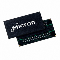
MT46H8M16LFCF-10 Micron Technology Inc, MT46H8M16LFCF-10 Datasheet - Page 13

MT46H8M16LFCF-10
Manufacturer Part Number
MT46H8M16LFCF-10
Description
IC DDR SDRAM 128MBIT 60VFBGA
Manufacturer
Micron Technology Inc
Type
DDR SDRAMr
Specifications of MT46H8M16LFCF-10
Format - Memory
RAM
Memory Type
Mobile DDR SDRAM
Memory Size
128M (8Mx16)
Speed
100MHz
Interface
Parallel
Voltage - Supply
1.7 V ~ 1.9 V
Operating Temperature
0°C ~ 70°C
Package / Case
60-VFBGA
Organization
8Mx16
Density
128Mb
Address Bus
15b
Access Time (max)
7ns
Maximum Clock Rate
104MHz
Operating Supply Voltage (typ)
1.8V
Package Type
VFBGA
Operating Temp Range
0C to 70C
Operating Supply Voltage (max)
1.9V
Operating Supply Voltage (min)
1.7V
Supply Current
90mA
Pin Count
60
Mounting
Surface Mount
Operating Temperature Classification
Commercial
Lead Free Status / RoHS Status
Lead free / RoHS Compliant
Available stocks
Company
Part Number
Manufacturer
Quantity
Price
Company:
Part Number:
MT46H8M16LFCF-10
Manufacturer:
Micron Technology Inc
Quantity:
10 000
Company:
Part Number:
MT46H8M16LFCF-10 IT
Manufacturer:
Micron Technology Inc
Quantity:
10 000
Company:
Part Number:
MT46H8M16LFCF-10 IT TR
Manufacturer:
Micron Technology Inc
Quantity:
10 000
Company:
Part Number:
MT46H8M16LFCF-10 TR
Manufacturer:
Micron Technology Inc
Quantity:
10 000
Partial-Array Self Refresh (PASR)
Output Driver Strength
Figure 5:
PDF: 09005aef822b7e27/Source: 09005aef822b7dd6
MT46H8M16LFB_2.fm - Rev. A 5/06 EN
E13
0
0
1
1
Extended Mode Register
E11
E12
0
–
0
1
0
1
Notes:
E10
Mode Register Definintion
Base Mode Register
Reserved
Extended Mode Register
Reserved
0
–
E9
0
–
E8
0
–
2. On-chip temperature sensor is used in place of TCSR. Setting these bits will have no effect.
For further power savings during SELF REFRESH, the PASR feature allows the controller
to select the amount of memory that will be refreshed during SELF REFRESH. The
refresh options are as follows:
• Full array: banks 0, 1, 2, and 3
• Half array: banks 0 and 1
• Quarter array: bank 0
WRITE and READ commands can still occur during standard operation, but only the
selected banks will be refreshed during SELF REFRESH. Data in banks that are disabled
will be lost.
Because the Mobile DDR SDRAM is designed for use in smaller systems that are mostly
point to point, an option to control the drive strength of the output buffers is available.
Drive strength should be selected based on the expected loading of the memory bus. Bits
A5 and A6 of the extended mode register can be used to select the driver strength of the
DQ outputs. There are three allowable settings for the output drivers (25 ohm internal
impedance, 55 ohm internal impedance, and 80 ohm internal impedance).
1. E13 and E12 (BA1 and BA0) must be “1, 0” to select the extended mode register (vs. the
13
1
BA1
E13
standard mode register).
1
E7
0
–
12
BA0
E12
0
1
Valid
–
11
A11
E11
set to “0”
10
A10
E10
Operating Mode
Normal Operation
All other states reserved
A9
E9
9
E6
0
0
1
1
A8
E8
8
E5
0
1
0
1
A7
E7
7
A6
E6
6
DS
13
5
A5
E5
TCSR
4
A4
E4
128Mb: 8 Meg x 16 Mobile DDR SDRAM
E2
0
0
0
0
1
1
1
1
Micron Technology, Inc., reserves the right to change products or specifications without notice.
2
A3
3
E3
E1
0
0
1
1
0
0
1
1
A2
2
E2
E0
0
1
0
1
0
1
0
1
PASR
A1
1
E1
Partial Array Self Refresh Coverage
Full Array (All Banks)
Half Array (BA1 = 0)
Quarter Array (BA1 = BA0 = 0)
Reserved
Reserved
Reserved
Reserved
Reserved
A0
0
E0
Address Bus
Extended Mode
Register
©2006 Micron Technology, Inc. All rights reserved.
Register Definition
Advance


