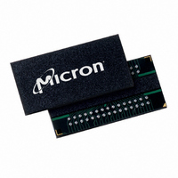
MT46H8M16LFCF-10 Micron Technology Inc, MT46H8M16LFCF-10 Datasheet - Page 40

MT46H8M16LFCF-10
Manufacturer Part Number
MT46H8M16LFCF-10
Description
IC DDR SDRAM 128MBIT 60VFBGA
Manufacturer
Micron Technology Inc
Type
DDR SDRAMr
Specifications of MT46H8M16LFCF-10
Format - Memory
RAM
Memory Type
Mobile DDR SDRAM
Memory Size
128M (8Mx16)
Speed
100MHz
Interface
Parallel
Voltage - Supply
1.7 V ~ 1.9 V
Operating Temperature
0°C ~ 70°C
Package / Case
60-VFBGA
Organization
8Mx16
Density
128Mb
Address Bus
15b
Access Time (max)
7ns
Maximum Clock Rate
104MHz
Operating Supply Voltage (typ)
1.8V
Package Type
VFBGA
Operating Temp Range
0C to 70C
Operating Supply Voltage (max)
1.9V
Operating Supply Voltage (min)
1.7V
Supply Current
90mA
Pin Count
60
Mounting
Surface Mount
Operating Temperature Classification
Commercial
Lead Free Status / RoHS Status
Lead free / RoHS Compliant
Available stocks
Company
Part Number
Manufacturer
Quantity
Price
Company:
Part Number:
MT46H8M16LFCF-10
Manufacturer:
Micron Technology Inc
Quantity:
10 000
Company:
Part Number:
MT46H8M16LFCF-10 IT
Manufacturer:
Micron Technology Inc
Quantity:
10 000
Company:
Part Number:
MT46H8M16LFCF-10 IT TR
Manufacturer:
Micron Technology Inc
Quantity:
10 000
Company:
Part Number:
MT46H8M16LFCF-10 TR
Manufacturer:
Micron Technology Inc
Quantity:
10 000
PRECHARGE
Figure 28:
Power-Down (CKE Not Active)
PDF: 09005aef822b7e27/Source: 09005aef822b7dd6
MT46H8M16LFB_2.fm - Rev. A 5/06 EN
PRECHARGE Command
Notes:
1. CA = Column Address.
The PRECHARGE command (see Figure 28) is used to deactivate the open row in a
particular bank or the open row in all banks. The bank(s) will be available for a subse-
quent row access some specified time (
Input A10 determines whether one or all banks are to be precharged, and in the case
where only one bank is to be precharged, inputs BA0, BA1 select the bank. When all
banks are to be precharged, inputs BA0, BA1 are treated as “Don’t Care.” Once a bank
has been precharged, it is in the idle state and must be activated prior to any READ or
WRITE commands being issued to that bank.
A0–A8
Unlike SDR SDRAMs, DDR SDRAMs require CKE to be active at all times an access is in
progress: from the issuing of a READ or WRITE command until completion of the burst;
thus a clock suspend is not supported. For READs, a burst completion is defined when
the read postamble is satisfied; for WRITEs, a burst completion is defined when the write
postamble is satisfied.
BA0,1
RAS#
CAS#
WE#
CKE
A11
A10
CK#
CS#
BA = Bank Address.
All = All banks to be Precharged, BA1, BA0 are “Don't Care.”
Single = Only bank selected by BA1 and BA0 will be precharged.
CK
HIGH
Single
DON’T CARE
All
BA
CA
40
128Mb: 8 Meg x 16 Mobile DDR SDRAM
Micron Technology, Inc., reserves the right to change products or specifications without notice.
t
RP) after the PRECHARGE command is issued.
©2006 Micron Technology, Inc. All rights reserved.
Operations
Advance


