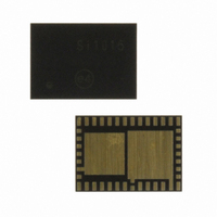
SI1014-A-GM Silicon Laboratories Inc, SI1014-A-GM Datasheet - Page 44

SI1014-A-GM
Manufacturer Part Number
SI1014-A-GM
Description
IC TXRX MCU + EZRADIOPRO
Manufacturer
Silicon Laboratories Inc
Specifications of SI1014-A-GM
Package / Case
42-QFN
Frequency
240MHz ~ 960MHz
Data Rate - Maximum
256kbps
Modulation Or Protocol
FSK, GFSK, OOK
Applications
General Purpose
Power - Output
13dBm
Sensitivity
-121dBm
Voltage - Supply
0.9 V ~ 3.6 V
Current - Receiving
18.5mA
Current - Transmitting
30mA
Data Interface
PCB, Surface Mount
Memory Size
16kB Flash, 768B RAM
Antenna Connector
PCB, Surface Mount
Number Of Receivers
1
Number Of Transmitters
1
Wireless Frequency
240 MHz to 960 MHz
Interface Type
UART, SMBus, SPI, PCA
Output Power
13 dBm
Operating Supply Voltage
0.9 V to 3.6 V
Maximum Operating Temperature
+ 85 C
Mounting Style
SMD/SMT
Maximum Supply Current
4 mA
Minimum Operating Temperature
- 40 C
Modulation
FSK, GFSK, OOK
Protocol Supported
C2, SMBus
Core
8051
Program Memory Type
Flash
Program Memory Size
16 KB
Data Ram Size
768 B
Supply Current (max)
4 mA
Lead Free Status / RoHS Status
Lead free / RoHS Compliant
Operating Temperature
-
Lead Free Status / Rohs Status
Lead free / RoHS Compliant
Other names
336-1869-5
Available stocks
Company
Part Number
Manufacturer
Quantity
Price
Company:
Part Number:
SI1014-A-GM
Manufacturer:
Silicon Laboratories Inc
Quantity:
135
- Current page: 44 of 384
- Download datasheet (3Mb)
Table 4.1. Absolute Maximum Ratings
Si1010/1/2/3/4/5
4. Electrical Characteristics
In Section 4.1 and Section 4.2, “V
to the VDD_MCU/DC+ supply voltage on Si1004/5 devices. The ADC, Comparator, and Port I/O specifica-
tions in these two sections do not apply to the EZRadioPRO peripheral.
In Section 4.3 and Section 4.4, “V
tions in these sections pertain to the EZRadioPRO peripheral.
4.1. Absolute Maximum Specifications
44
Ambient temperature under bias
Storage Temperature
Voltage on any Px.x I/O Pin or
RST with Respect to GND
Voltage on VBAT with respect to
GND
Voltage on VDD_MCU or
VDD_MCU/DC+ with respect to
GND
Maximum Total Current through
VBAT, DCEN, VDD_MCU/DC+ or
GND
Maximum Output Current Sunk
by RST or any Px.x Pin
Maximum Total Current through
all Px.x Pins
DC-DC Converter Output Power
ESD (Human Body Model)
ESD (Machine Model)
Note: Stresses above those listed under “Absolute Maximum Ratings” may cause permanent damage to the device.
This is a stress rating only and functional operation of the devices at those or any other conditions above those
indicated in the operation listings of this specification is not implied. Exposure to maximum rating conditions for
extended periods may affect device reliability.
Parameter
DD
DD
VDD > 2.2 V
VDD < 2.2 V
One-Cell Mode
Two-Cell Mode
All pins except TX, RXp,
and RXn
TX, RXp, and RXn
All pins except TX, RXp,
and RXn
TX, RXp, and RXn
” refers to the VDD_MCU supply voltage on Si1010/1/2/3 devices and
” refers to the VDD_RF and VDD_DIG Supply Voltage. All specifica-
Conditions
Rev. 1.0
–0.3
–0.3
–0.3
–0.3
–0.3
Min
–55
–65
—
—
—
—
—
—
—
—
Typ
—
—
—
—
—
—
—
—
—
—
—
—
—
—
—
VDD + 3.6
Max
125
150
500
100
200
150
110
5.8
4.0
4.0
4.0
45
2
1
Units
mW
mA
mA
mA
kV
kV
°C
°C
V
V
V
V
V
Related parts for SI1014-A-GM
Image
Part Number
Description
Manufacturer
Datasheet
Request
R
Part Number:
Description:
QFN 42/I�/16KB, 768B RAM, +13 DBM, PROGRAMMABLE XCVR, DC-DC
Manufacturer:
Silicon Laboratories Inc
Part Number:
Description:
SMD/C�/SINGLE-ENDED OUTPUT SILICON OSCILLATOR
Manufacturer:
Silicon Laboratories Inc
Part Number:
Description:
Manufacturer:
Silicon Laboratories Inc
Datasheet:
Part Number:
Description:
N/A N/A/SI4010 AES KEYFOB DEMO WITH LCD RX
Manufacturer:
Silicon Laboratories Inc
Datasheet:
Part Number:
Description:
N/A N/A/SI4010 SIMPLIFIED KEY FOB DEMO WITH LED RX
Manufacturer:
Silicon Laboratories Inc
Datasheet:
Part Number:
Description:
N/A/-40 TO 85 OC/EZLINK MODULE; F930/4432 HIGH BAND (REV E/B1)
Manufacturer:
Silicon Laboratories Inc
Part Number:
Description:
EZLink Module; F930/4432 Low Band (rev e/B1)
Manufacturer:
Silicon Laboratories Inc
Part Number:
Description:
I�/4460 10 DBM RADIO TEST CARD 434 MHZ
Manufacturer:
Silicon Laboratories Inc
Part Number:
Description:
I�/4461 14 DBM RADIO TEST CARD 868 MHZ
Manufacturer:
Silicon Laboratories Inc
Part Number:
Description:
I�/4463 20 DBM RFSWITCH RADIO TEST CARD 460 MHZ
Manufacturer:
Silicon Laboratories Inc
Part Number:
Description:
I�/4463 20 DBM RADIO TEST CARD 868 MHZ
Manufacturer:
Silicon Laboratories Inc
Part Number:
Description:
I�/4463 27 DBM RADIO TEST CARD 868 MHZ
Manufacturer:
Silicon Laboratories Inc
Part Number:
Description:
I�/4463 SKYWORKS 30 DBM RADIO TEST CARD 915 MHZ
Manufacturer:
Silicon Laboratories Inc
Part Number:
Description:
N/A N/A/-40 TO 85 OC/4463 RFMD 30 DBM RADIO TEST CARD 915 MHZ
Manufacturer:
Silicon Laboratories Inc


