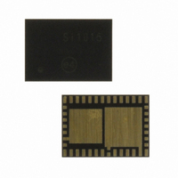
SI1014-A-GM Silicon Laboratories Inc, SI1014-A-GM Datasheet - Page 144

SI1014-A-GM
Manufacturer Part Number
SI1014-A-GM
Description
IC TXRX MCU + EZRADIOPRO
Manufacturer
Silicon Laboratories Inc
Specifications of SI1014-A-GM
Package / Case
42-QFN
Frequency
240MHz ~ 960MHz
Data Rate - Maximum
256kbps
Modulation Or Protocol
FSK, GFSK, OOK
Applications
General Purpose
Power - Output
13dBm
Sensitivity
-121dBm
Voltage - Supply
0.9 V ~ 3.6 V
Current - Receiving
18.5mA
Current - Transmitting
30mA
Data Interface
PCB, Surface Mount
Memory Size
16kB Flash, 768B RAM
Antenna Connector
PCB, Surface Mount
Number Of Receivers
1
Number Of Transmitters
1
Wireless Frequency
240 MHz to 960 MHz
Interface Type
UART, SMBus, SPI, PCA
Output Power
13 dBm
Operating Supply Voltage
0.9 V to 3.6 V
Maximum Operating Temperature
+ 85 C
Mounting Style
SMD/SMT
Maximum Supply Current
4 mA
Minimum Operating Temperature
- 40 C
Modulation
FSK, GFSK, OOK
Protocol Supported
C2, SMBus
Core
8051
Program Memory Type
Flash
Program Memory Size
16 KB
Data Ram Size
768 B
Supply Current (max)
4 mA
Lead Free Status / RoHS Status
Lead free / RoHS Compliant
Operating Temperature
-
Lead Free Status / Rohs Status
Lead free / RoHS Compliant
Other names
336-1869-5
Available stocks
Company
Part Number
Manufacturer
Quantity
Price
Company:
Part Number:
SI1014-A-GM
Manufacturer:
Silicon Laboratories Inc
Quantity:
135
- Current page: 144 of 384
- Download datasheet (3Mb)
Si1010/1/2/3/4/5
12.6. External Interrupts INT0 and INT1
The INT0 and INT1 external interrupt sources are configurable as active high or low, edge or level sensi-
tive. The IN0PL (INT0 Polarity) and IN1PL (INT1 Polarity) bits in the IT01CF register select active high or
active low; the IT0 and IT1 bits in TCON (Section “27.1. Timer 0 and Timer 1” on page 340) select level or
edge sensitive. The table below lists the possible configurations.
INT0 and INT1 are assigned to Port pins as defined in the IT01CF register (see SFR Definition 12.7). Note
that INT0 and INT0 Port pin assignments are independent of any Crossbar assignments. INT0 and INT1
will monitor their assigned Port pins without disturbing the peripheral that was assigned the Port pin via the
Crossbar. To assign a Port pin only to INT0 and/or INT1, configure the Crossbar to skip the selected pin(s).
This is accomplished by setting the associated bit in register XBR0 (see Section “21.3. Priority Crossbar
Decoder” on page 223 for complete details on configuring the Crossbar).
IE0 (TCON.1) and IE1 (TCON.3) serve as the interrupt-pending flags for the INT0 and INT1 external inter-
rupts, respectively. If an INT0 or INT1 external interrupt is configured as edge-sensitive, the corresponding
interrupt-pending flag is automatically cleared by the hardware when the CPU vectors to the ISR. When
configured as level sensitive, the interrupt-pending flag remains logic 1 while the input is active as defined
by the corresponding polarity bit (IN0PL or IN1PL); the flag remains logic 0 while the input is inactive. The
external interrupt source must hold the input active until the interrupt request is recognized. It must then
deactivate the interrupt request before execution of the ISR completes or another interrupt request will be
generated.
144
IT0
1
1
0
0
IN0PL
0
1
0
1
INT0 Interrupt
Active low, edge sensitive
Active high, edge sensitive
Active low, level sensitive
Active high, level sensitive
Rev. 1.0
IT1
1
1
0
0
IN1PL
0
1
0
1
INT1 Interrupt
Active low, edge sensitive
Active high, edge sensitive
Active low, level sensitive
Active high, level sensitive
Related parts for SI1014-A-GM
Image
Part Number
Description
Manufacturer
Datasheet
Request
R
Part Number:
Description:
QFN 42/I�/16KB, 768B RAM, +13 DBM, PROGRAMMABLE XCVR, DC-DC
Manufacturer:
Silicon Laboratories Inc
Part Number:
Description:
SMD/C�/SINGLE-ENDED OUTPUT SILICON OSCILLATOR
Manufacturer:
Silicon Laboratories Inc
Part Number:
Description:
Manufacturer:
Silicon Laboratories Inc
Datasheet:
Part Number:
Description:
N/A N/A/SI4010 AES KEYFOB DEMO WITH LCD RX
Manufacturer:
Silicon Laboratories Inc
Datasheet:
Part Number:
Description:
N/A N/A/SI4010 SIMPLIFIED KEY FOB DEMO WITH LED RX
Manufacturer:
Silicon Laboratories Inc
Datasheet:
Part Number:
Description:
N/A/-40 TO 85 OC/EZLINK MODULE; F930/4432 HIGH BAND (REV E/B1)
Manufacturer:
Silicon Laboratories Inc
Part Number:
Description:
EZLink Module; F930/4432 Low Band (rev e/B1)
Manufacturer:
Silicon Laboratories Inc
Part Number:
Description:
I�/4460 10 DBM RADIO TEST CARD 434 MHZ
Manufacturer:
Silicon Laboratories Inc
Part Number:
Description:
I�/4461 14 DBM RADIO TEST CARD 868 MHZ
Manufacturer:
Silicon Laboratories Inc
Part Number:
Description:
I�/4463 20 DBM RFSWITCH RADIO TEST CARD 460 MHZ
Manufacturer:
Silicon Laboratories Inc
Part Number:
Description:
I�/4463 20 DBM RADIO TEST CARD 868 MHZ
Manufacturer:
Silicon Laboratories Inc
Part Number:
Description:
I�/4463 27 DBM RADIO TEST CARD 868 MHZ
Manufacturer:
Silicon Laboratories Inc
Part Number:
Description:
I�/4463 SKYWORKS 30 DBM RADIO TEST CARD 915 MHZ
Manufacturer:
Silicon Laboratories Inc
Part Number:
Description:
N/A N/A/-40 TO 85 OC/4463 RFMD 30 DBM RADIO TEST CARD 915 MHZ
Manufacturer:
Silicon Laboratories Inc


