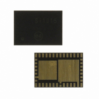
SI1014-A-GM Silicon Laboratories Inc, SI1014-A-GM Datasheet - Page 280

SI1014-A-GM
Manufacturer Part Number
SI1014-A-GM
Description
IC TXRX MCU + EZRADIOPRO
Manufacturer
Silicon Laboratories Inc
Specifications of SI1014-A-GM
Package / Case
42-QFN
Frequency
240MHz ~ 960MHz
Data Rate - Maximum
256kbps
Modulation Or Protocol
FSK, GFSK, OOK
Applications
General Purpose
Power - Output
13dBm
Sensitivity
-121dBm
Voltage - Supply
0.9 V ~ 3.6 V
Current - Receiving
18.5mA
Current - Transmitting
30mA
Data Interface
PCB, Surface Mount
Memory Size
16kB Flash, 768B RAM
Antenna Connector
PCB, Surface Mount
Number Of Receivers
1
Number Of Transmitters
1
Wireless Frequency
240 MHz to 960 MHz
Interface Type
UART, SMBus, SPI, PCA
Output Power
13 dBm
Operating Supply Voltage
0.9 V to 3.6 V
Maximum Operating Temperature
+ 85 C
Mounting Style
SMD/SMT
Maximum Supply Current
4 mA
Minimum Operating Temperature
- 40 C
Modulation
FSK, GFSK, OOK
Protocol Supported
C2, SMBus
Core
8051
Program Memory Type
Flash
Program Memory Size
16 KB
Data Ram Size
768 B
Supply Current (max)
4 mA
Lead Free Status / RoHS Status
Lead free / RoHS Compliant
Operating Temperature
-
Lead Free Status / Rohs Status
Lead free / RoHS Compliant
Other names
336-1869-5
Available stocks
Company
Part Number
Manufacturer
Quantity
Price
Company:
Part Number:
SI1014-A-GM
Manufacturer:
Silicon Laboratories Inc
Quantity:
135
- Current page: 280 of 384
- Download datasheet (3Mb)
Si1010/1/2/3/4/5
The reset will initialize all registers to their default values. The reset signal is also available for output and
use by the microcontroller by using the default setting for GPIO_0. The inverted reset signal is available by
default on GPIO_1.
23.8.2. Output Clock
The 30 MHz crystal oscillator frequency is divided down internally and may be output on GPIO2. This fea-
ture is useful to lower BOM cost by using only one crystal in the system. The output clock on GPIO2 may
be routed to the XTAL2 input to provide a synchronized clock source between the MCU and the EZRadio-
PRO peripheral. The output clock frequency is selectable from one of 8 options, as shown below. Except
for the 32.768 kHz option, all other frequencies are derived by dividing the crystal oscillator frequency. The
32.768 kHz clock signal is derived from an internal RC oscillator or an external 32 kHz crystal. The default
setting for GPIO2 is to output the clock signal with a frequency of 1 MHz.
Since the crystal oscillator is disabled in SLEEP mode in order to save current, the low-power 32.768 kHz
clock can be automatically switched to become the output clock. This feature is called enable low fre-
quency clock and is enabled by the enlfc bit in “Register 0Ah. Microcontroller Output Clock." When enlfc =
1 and the chip is in SLEEP mode then the 32.768 kHz clock will be provided regardless of the setting of
mclk[2:0]. For example, if mclk[2:0] = 000, 30 MHz will be provided through the GPIO output pin in all IDLE,
280
Release Reset Voltage
Power-On V
Low V
Software Reset Pulse
Threshold Voltage
Reference Slope
V
Add R/W
0A
DD
Glitch Reset Pulse
R/W
DD
Parameter
Limit
DD
Slope
Description
Output Clock
Function/
TSWRST
Symbol
SVDD
VTSD
VRR
VLD
TP
k
D7
Table 23.6. POR Parameters
mclk[2:0]
000
001
010
011
100
101
110
111
D6
Also occurs after SDN, and
VLD<VRR is guaranteed
tested V
Rev. 1.0
clkt[1]
initial power on
D5
Modulation Source
Comment
DD
32.768 kHz
clkt[0]
slope region
D4
30 MHz
15 MHz
10 MHz
4 MHz
3 MHz
2 MHz
1 MHz
enlfc
D3
mclk[2] mclk[1] mclk[0]
D2
0.85
0.03
Min
0.7
50
—
—
5
D1
Typ
1.3
0.4
0.2
16
—
—
1
D0
Max
1.75
300
470
1.3
25
—
—
POR Def.
06h
V/ms
V/ms
Unit
ms
us
V
V
V
Related parts for SI1014-A-GM
Image
Part Number
Description
Manufacturer
Datasheet
Request
R
Part Number:
Description:
QFN 42/I�/16KB, 768B RAM, +13 DBM, PROGRAMMABLE XCVR, DC-DC
Manufacturer:
Silicon Laboratories Inc
Part Number:
Description:
SMD/C�/SINGLE-ENDED OUTPUT SILICON OSCILLATOR
Manufacturer:
Silicon Laboratories Inc
Part Number:
Description:
Manufacturer:
Silicon Laboratories Inc
Datasheet:
Part Number:
Description:
N/A N/A/SI4010 AES KEYFOB DEMO WITH LCD RX
Manufacturer:
Silicon Laboratories Inc
Datasheet:
Part Number:
Description:
N/A N/A/SI4010 SIMPLIFIED KEY FOB DEMO WITH LED RX
Manufacturer:
Silicon Laboratories Inc
Datasheet:
Part Number:
Description:
N/A/-40 TO 85 OC/EZLINK MODULE; F930/4432 HIGH BAND (REV E/B1)
Manufacturer:
Silicon Laboratories Inc
Part Number:
Description:
EZLink Module; F930/4432 Low Band (rev e/B1)
Manufacturer:
Silicon Laboratories Inc
Part Number:
Description:
I�/4460 10 DBM RADIO TEST CARD 434 MHZ
Manufacturer:
Silicon Laboratories Inc
Part Number:
Description:
I�/4461 14 DBM RADIO TEST CARD 868 MHZ
Manufacturer:
Silicon Laboratories Inc
Part Number:
Description:
I�/4463 20 DBM RFSWITCH RADIO TEST CARD 460 MHZ
Manufacturer:
Silicon Laboratories Inc
Part Number:
Description:
I�/4463 20 DBM RADIO TEST CARD 868 MHZ
Manufacturer:
Silicon Laboratories Inc
Part Number:
Description:
I�/4463 27 DBM RADIO TEST CARD 868 MHZ
Manufacturer:
Silicon Laboratories Inc
Part Number:
Description:
I�/4463 SKYWORKS 30 DBM RADIO TEST CARD 915 MHZ
Manufacturer:
Silicon Laboratories Inc
Part Number:
Description:
N/A N/A/-40 TO 85 OC/4463 RFMD 30 DBM RADIO TEST CARD 915 MHZ
Manufacturer:
Silicon Laboratories Inc


