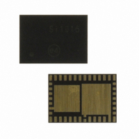
SI1014-A-GM Silicon Laboratories Inc, SI1014-A-GM Datasheet - Page 219

SI1014-A-GM
Manufacturer Part Number
SI1014-A-GM
Description
IC TXRX MCU + EZRADIOPRO
Manufacturer
Silicon Laboratories Inc
Specifications of SI1014-A-GM
Package / Case
42-QFN
Frequency
240MHz ~ 960MHz
Data Rate - Maximum
256kbps
Modulation Or Protocol
FSK, GFSK, OOK
Applications
General Purpose
Power - Output
13dBm
Sensitivity
-121dBm
Voltage - Supply
0.9 V ~ 3.6 V
Current - Receiving
18.5mA
Current - Transmitting
30mA
Data Interface
PCB, Surface Mount
Memory Size
16kB Flash, 768B RAM
Antenna Connector
PCB, Surface Mount
Number Of Receivers
1
Number Of Transmitters
1
Wireless Frequency
240 MHz to 960 MHz
Interface Type
UART, SMBus, SPI, PCA
Output Power
13 dBm
Operating Supply Voltage
0.9 V to 3.6 V
Maximum Operating Temperature
+ 85 C
Mounting Style
SMD/SMT
Maximum Supply Current
4 mA
Minimum Operating Temperature
- 40 C
Modulation
FSK, GFSK, OOK
Protocol Supported
C2, SMBus
Core
8051
Program Memory Type
Flash
Program Memory Size
16 KB
Data Ram Size
768 B
Supply Current (max)
4 mA
Lead Free Status / RoHS Status
Lead free / RoHS Compliant
Operating Temperature
-
Lead Free Status / Rohs Status
Lead free / RoHS Compliant
Other names
336-1869-5
Available stocks
Company
Part Number
Manufacturer
Quantity
Price
Company:
Part Number:
SI1014-A-GM
Manufacturer:
Silicon Laboratories Inc
Quantity:
135
- Current page: 219 of 384
- Download datasheet (3Mb)
21. Port Input/Output
Digital and analog resources are available through 12 I/O pins. Port pins are organized as three byte-wide
ports. Port pins P0.0–P1.6 can be defined as digital or analog I/O. Digital I/O pins can be assigned to one
of the internal digital resources or used as general purpose I/O (GPIO). Analog I/O pins are used by the
internal analog resources. P1.0, P1.1, P1.2, and P1.3 are dedicated for communication with the EZRadio-
PRO peripheral. P2.7 can be used as GPIO and is shared with the C2 Interface Data signal (C2D). See
Section “29. C2 Interface” on page 379 for more details.
The designer has complete control over which digital and analog functions are assigned to individual Port
pins, limited only by the number of physical I/O pins. This resource assignment flexibility is achieved
through the use of a Priority Crossbar Decoder. See Section 21.3 for more information on the Crossbar.
All Px.x Port I/Os are 5 V tolerant when used as digital inputs or open-drain outputs. For Port I/Os config-
ured as push-pull outputs, current is sourced from the VDD_MCU/DC+ supply. Port I/Os used for analog
functions can operate up to the VDD_MCU/DC+ supply voltage. See Section 21.1 for more information on
Port I/O operating modes and the electrical specifications chapter for detailed electrical specifications.
Highest
Priority
Lowest
Priority
SYSCLK
Outputs
SMBus
T0, T1
UART
P0
P1
P2
SPI0
SPI1
CP0
CP1
PCA
(P0.0-P0.7)
(P1.0-P1.6)
(P2.7)
Figure 21.1. Port I/O Functional Block Diagram
2
4
2
4
7
2
8
7
1
(ADC0, CP0, and CP1 inputs,
Note: P1.0, P1.1, P1.2, and P1.3 are internally
connected to the EZRadioPRO peripheral.
To Analog Peripherals
Rev. 1.0
VREF, IREF0, AGND)
XBR2, PnSKIP
XBR0, XBR1,
Crossbar
Decoder
Registers
Priority
Digital
8
7
1
P0MASK, P0MAT
P1MASK, P1MAT
Port Match
Si1010/1/2/3/4/5
Cells
Cells
Cell
I/O
I/O
I/O
P0
P1
P2
PnMDIN Registers
External Interrupts
EX0 and EX1
PnMDOUT,
No analog functionality
available on P2.7
P0.0
P0.7
P1.4
P1.5
P1.6
P2.7
219
Related parts for SI1014-A-GM
Image
Part Number
Description
Manufacturer
Datasheet
Request
R
Part Number:
Description:
QFN 42/I�/16KB, 768B RAM, +13 DBM, PROGRAMMABLE XCVR, DC-DC
Manufacturer:
Silicon Laboratories Inc
Part Number:
Description:
SMD/C�/SINGLE-ENDED OUTPUT SILICON OSCILLATOR
Manufacturer:
Silicon Laboratories Inc
Part Number:
Description:
Manufacturer:
Silicon Laboratories Inc
Datasheet:
Part Number:
Description:
N/A N/A/SI4010 AES KEYFOB DEMO WITH LCD RX
Manufacturer:
Silicon Laboratories Inc
Datasheet:
Part Number:
Description:
N/A N/A/SI4010 SIMPLIFIED KEY FOB DEMO WITH LED RX
Manufacturer:
Silicon Laboratories Inc
Datasheet:
Part Number:
Description:
N/A/-40 TO 85 OC/EZLINK MODULE; F930/4432 HIGH BAND (REV E/B1)
Manufacturer:
Silicon Laboratories Inc
Part Number:
Description:
EZLink Module; F930/4432 Low Band (rev e/B1)
Manufacturer:
Silicon Laboratories Inc
Part Number:
Description:
I�/4460 10 DBM RADIO TEST CARD 434 MHZ
Manufacturer:
Silicon Laboratories Inc
Part Number:
Description:
I�/4461 14 DBM RADIO TEST CARD 868 MHZ
Manufacturer:
Silicon Laboratories Inc
Part Number:
Description:
I�/4463 20 DBM RFSWITCH RADIO TEST CARD 460 MHZ
Manufacturer:
Silicon Laboratories Inc
Part Number:
Description:
I�/4463 20 DBM RADIO TEST CARD 868 MHZ
Manufacturer:
Silicon Laboratories Inc
Part Number:
Description:
I�/4463 27 DBM RADIO TEST CARD 868 MHZ
Manufacturer:
Silicon Laboratories Inc
Part Number:
Description:
I�/4463 SKYWORKS 30 DBM RADIO TEST CARD 915 MHZ
Manufacturer:
Silicon Laboratories Inc
Part Number:
Description:
N/A N/A/-40 TO 85 OC/4463 RFMD 30 DBM RADIO TEST CARD 915 MHZ
Manufacturer:
Silicon Laboratories Inc


