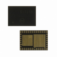
SI1014-A-GM Silicon Laboratories Inc, SI1014-A-GM Datasheet - Page 33

SI1014-A-GM
Manufacturer Part Number
SI1014-A-GM
Description
IC TXRX MCU + EZRADIOPRO
Manufacturer
Silicon Laboratories Inc
Specifications of SI1014-A-GM
Package / Case
42-QFN
Frequency
240MHz ~ 960MHz
Data Rate - Maximum
256kbps
Modulation Or Protocol
FSK, GFSK, OOK
Applications
General Purpose
Power - Output
13dBm
Sensitivity
-121dBm
Voltage - Supply
0.9 V ~ 3.6 V
Current - Receiving
18.5mA
Current - Transmitting
30mA
Data Interface
PCB, Surface Mount
Memory Size
16kB Flash, 768B RAM
Antenna Connector
PCB, Surface Mount
Number Of Receivers
1
Number Of Transmitters
1
Wireless Frequency
240 MHz to 960 MHz
Interface Type
UART, SMBus, SPI, PCA
Output Power
13 dBm
Operating Supply Voltage
0.9 V to 3.6 V
Maximum Operating Temperature
+ 85 C
Mounting Style
SMD/SMT
Maximum Supply Current
4 mA
Minimum Operating Temperature
- 40 C
Modulation
FSK, GFSK, OOK
Protocol Supported
C2, SMBus
Core
8051
Program Memory Type
Flash
Program Memory Size
16 KB
Data Ram Size
768 B
Supply Current (max)
4 mA
Lead Free Status / RoHS Status
Lead free / RoHS Compliant
Operating Temperature
-
Lead Free Status / Rohs Status
Lead free / RoHS Compliant
Other names
336-1869-5
Available stocks
Company
Part Number
Manufacturer
Quantity
Price
Company:
Part Number:
SI1014-A-GM
Manufacturer:
Silicon Laboratories Inc
Quantity:
135
- Current page: 33 of 384
- Download datasheet (3Mb)
XTAL3
XTAL4
XTAL1
XTAL2
AGND
Name
C2CK
P2.7/
RST/
V
P0.0
P0.1
P0.2
P0.3
C2D
REF
Si1010/1
Si1012/3
Table 3.1. Pin Definitions for the Si1010/1/2/3/4/5 (Continued)
Pin Number
39
40
42
36
35
34
33
1
Si1014/5
42
36
35
34
33
1
3
2
D I/O or
D I/O or
D I/O or
D I/O or
A Out
A Out
A Out
D I/O
D I/O
D I/O
D I/O
Type
D In
A In
A In
A In
A In
A In
A In
A In
A In
G
Device Reset. Open-drain output of internal POR or V
monitor. An external source can initiate a system reset by
driving this pin low for at least 15 µs. A 1–5 k pullup to
VDD_MCU is recommended. See Reset Sources section
for a complete description.
Clock signal for the C2 Debug Interface.
Port 2.7. This pin can only be used as GPIO. The Crossbar
cannot route signals to this pin and it cannot be configured
as an analog input. See Port I/O section for a complete
description.
Bi-directional data signal for the C2 Debug Interface.
SmaRTClock Oscillator Crystal Input.
See Section 20 for a complete description.
SmaRTClock Oscillator Crystal Output.
See Section 20 for a complete description.
Port 0.0. See Port I/O section for a complete description.
External V
Internal V
are recommended. See Voltage Reference section.
Port 0.1. See Port I/O Section for a complete description.
Optional Analog Ground. See VREF chapter.
Port 0.2. See Port I/O Section for a complete description.
External Clock Input. This pin is the external oscillator
return for a crystal or resonator. See Oscillator section.
Port 0.3. See Port I/O Section for a complete description.
External Clock Output. This pin is the excitation driver for an
external crystal or resonator.
External Clock Input. This pin is the external clock input in
external CMOS clock mode.
External Clock Input. This pin is the external clock input in
capacitor or RC oscillator configurations.
See Oscillator section for complete details.
Rev. 1.0
REF
REF
Output. External V
Input.
Description
Si1010/1/2/3/4/5
REF
decoupling capacitors
DD
33
Related parts for SI1014-A-GM
Image
Part Number
Description
Manufacturer
Datasheet
Request
R
Part Number:
Description:
QFN 42/I�/16KB, 768B RAM, +13 DBM, PROGRAMMABLE XCVR, DC-DC
Manufacturer:
Silicon Laboratories Inc
Part Number:
Description:
SMD/C�/SINGLE-ENDED OUTPUT SILICON OSCILLATOR
Manufacturer:
Silicon Laboratories Inc
Part Number:
Description:
Manufacturer:
Silicon Laboratories Inc
Datasheet:
Part Number:
Description:
N/A N/A/SI4010 AES KEYFOB DEMO WITH LCD RX
Manufacturer:
Silicon Laboratories Inc
Datasheet:
Part Number:
Description:
N/A N/A/SI4010 SIMPLIFIED KEY FOB DEMO WITH LED RX
Manufacturer:
Silicon Laboratories Inc
Datasheet:
Part Number:
Description:
N/A/-40 TO 85 OC/EZLINK MODULE; F930/4432 HIGH BAND (REV E/B1)
Manufacturer:
Silicon Laboratories Inc
Part Number:
Description:
EZLink Module; F930/4432 Low Band (rev e/B1)
Manufacturer:
Silicon Laboratories Inc
Part Number:
Description:
I�/4460 10 DBM RADIO TEST CARD 434 MHZ
Manufacturer:
Silicon Laboratories Inc
Part Number:
Description:
I�/4461 14 DBM RADIO TEST CARD 868 MHZ
Manufacturer:
Silicon Laboratories Inc
Part Number:
Description:
I�/4463 20 DBM RFSWITCH RADIO TEST CARD 460 MHZ
Manufacturer:
Silicon Laboratories Inc
Part Number:
Description:
I�/4463 20 DBM RADIO TEST CARD 868 MHZ
Manufacturer:
Silicon Laboratories Inc
Part Number:
Description:
I�/4463 27 DBM RADIO TEST CARD 868 MHZ
Manufacturer:
Silicon Laboratories Inc
Part Number:
Description:
I�/4463 SKYWORKS 30 DBM RADIO TEST CARD 915 MHZ
Manufacturer:
Silicon Laboratories Inc
Part Number:
Description:
N/A N/A/-40 TO 85 OC/4463 RFMD 30 DBM RADIO TEST CARD 915 MHZ
Manufacturer:
Silicon Laboratories Inc


