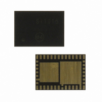
SI1014-A-GM Silicon Laboratories Inc, SI1014-A-GM Datasheet - Page 262

SI1014-A-GM
Manufacturer Part Number
SI1014-A-GM
Description
IC TXRX MCU + EZRADIOPRO
Manufacturer
Silicon Laboratories Inc
Specifications of SI1014-A-GM
Package / Case
42-QFN
Frequency
240MHz ~ 960MHz
Data Rate - Maximum
256kbps
Modulation Or Protocol
FSK, GFSK, OOK
Applications
General Purpose
Power - Output
13dBm
Sensitivity
-121dBm
Voltage - Supply
0.9 V ~ 3.6 V
Current - Receiving
18.5mA
Current - Transmitting
30mA
Data Interface
PCB, Surface Mount
Memory Size
16kB Flash, 768B RAM
Antenna Connector
PCB, Surface Mount
Number Of Receivers
1
Number Of Transmitters
1
Wireless Frequency
240 MHz to 960 MHz
Interface Type
UART, SMBus, SPI, PCA
Output Power
13 dBm
Operating Supply Voltage
0.9 V to 3.6 V
Maximum Operating Temperature
+ 85 C
Mounting Style
SMD/SMT
Maximum Supply Current
4 mA
Minimum Operating Temperature
- 40 C
Modulation
FSK, GFSK, OOK
Protocol Supported
C2, SMBus
Core
8051
Program Memory Type
Flash
Program Memory Size
16 KB
Data Ram Size
768 B
Supply Current (max)
4 mA
Lead Free Status / RoHS Status
Lead free / RoHS Compliant
Operating Temperature
-
Lead Free Status / Rohs Status
Lead free / RoHS Compliant
Other names
336-1869-5
Available stocks
Company
Part Number
Manufacturer
Quantity
Price
Company:
Part Number:
SI1014-A-GM
Manufacturer:
Silicon Laboratories Inc
Quantity:
135
- Current page: 262 of 384
- Download datasheet (3Mb)
Si1010/1/2/3/4/5
23.4.2. Modulation Data Source
The transceiver may be configured to obtain its modulation data from one of three different sources: FIFO
mode, Direct Mode, and from a PN9 mode. In Direct Mode, the TX modulation data may be obtained from
several different input pins. These options are set through the dtmod[1:0] field in "Register 71h. Modulation
Mode Control 2".
23.4.2.1. FIFO Mode
In FIFO mode, the transmit and receive data is stored in integrated FIFO register memory. The FIFOs are
accessed via "Register 7Fh. FIFO Access," and are most efficiently accessed with burst read/write opera-
tion.
In TX mode, the data bytes stored in FIFO memory are "packaged" together with other fields and bytes of
information to construct the final transmit packet structure. These other potential fields include the Pream-
ble, Sync word, Header, CRC checksum, etc. The configuration of the packet structure in TX mode is
262
Add R/W
dtmod[1:0]
71
TX Modulation Time Domain Waveforms -- FSK vs. GFSK
-0.5
-1.0
-1.5
-0.5
-1.0
1.5
1.0
0.5
0.0
1.0
0.5
0.0
00
01
10
11
R/W
0
50
Description
Function/
Modulation
100
Direct Mode using TX/RX Data via GPIO pin (GPIO configuration required)
Direct Mode using TX/RX Data via SDI pin (only when nSEL is high)
FIFO Mode
PN9 (internally generated)
Control 2
Mode
150
200
time, usec
250
trclk[1] trclk[0] dtmod[1] dtmod[0] eninv fd[8] modtyp[1] modtyp[0]
Figure 23.6. FSK vs. GFSK Spectrums
D7
300
350
D6
400
450
D5
500
Rev. 1.0
Data Source
-100
-100
TX Modulation Spectrum -- FSK vs GFSK (Continuous PRBS)
-20
-40
-60
-80
-20
-40
-60
-80
D4
-250
DataRate
-200
64000.0
D3
-150
-100
D2
TxDev
32000.0
-50
freq, KHz
D1
0
BT_Filter
50
0.5
100
D0
ModIndex
150
1.0
200
POR Def.
00h
250
Related parts for SI1014-A-GM
Image
Part Number
Description
Manufacturer
Datasheet
Request
R
Part Number:
Description:
QFN 42/I�/16KB, 768B RAM, +13 DBM, PROGRAMMABLE XCVR, DC-DC
Manufacturer:
Silicon Laboratories Inc
Part Number:
Description:
SMD/C�/SINGLE-ENDED OUTPUT SILICON OSCILLATOR
Manufacturer:
Silicon Laboratories Inc
Part Number:
Description:
Manufacturer:
Silicon Laboratories Inc
Datasheet:
Part Number:
Description:
N/A N/A/SI4010 AES KEYFOB DEMO WITH LCD RX
Manufacturer:
Silicon Laboratories Inc
Datasheet:
Part Number:
Description:
N/A N/A/SI4010 SIMPLIFIED KEY FOB DEMO WITH LED RX
Manufacturer:
Silicon Laboratories Inc
Datasheet:
Part Number:
Description:
N/A/-40 TO 85 OC/EZLINK MODULE; F930/4432 HIGH BAND (REV E/B1)
Manufacturer:
Silicon Laboratories Inc
Part Number:
Description:
EZLink Module; F930/4432 Low Band (rev e/B1)
Manufacturer:
Silicon Laboratories Inc
Part Number:
Description:
I�/4460 10 DBM RADIO TEST CARD 434 MHZ
Manufacturer:
Silicon Laboratories Inc
Part Number:
Description:
I�/4461 14 DBM RADIO TEST CARD 868 MHZ
Manufacturer:
Silicon Laboratories Inc
Part Number:
Description:
I�/4463 20 DBM RFSWITCH RADIO TEST CARD 460 MHZ
Manufacturer:
Silicon Laboratories Inc
Part Number:
Description:
I�/4463 20 DBM RADIO TEST CARD 868 MHZ
Manufacturer:
Silicon Laboratories Inc
Part Number:
Description:
I�/4463 27 DBM RADIO TEST CARD 868 MHZ
Manufacturer:
Silicon Laboratories Inc
Part Number:
Description:
I�/4463 SKYWORKS 30 DBM RADIO TEST CARD 915 MHZ
Manufacturer:
Silicon Laboratories Inc
Part Number:
Description:
N/A N/A/-40 TO 85 OC/4463 RFMD 30 DBM RADIO TEST CARD 915 MHZ
Manufacturer:
Silicon Laboratories Inc


