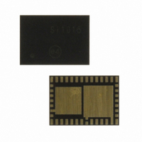
SI1014-A-GM Silicon Laboratories Inc, SI1014-A-GM Datasheet - Page 281

SI1014-A-GM
Manufacturer Part Number
SI1014-A-GM
Description
IC TXRX MCU + EZRADIOPRO
Manufacturer
Silicon Laboratories Inc
Specifications of SI1014-A-GM
Package / Case
42-QFN
Frequency
240MHz ~ 960MHz
Data Rate - Maximum
256kbps
Modulation Or Protocol
FSK, GFSK, OOK
Applications
General Purpose
Power - Output
13dBm
Sensitivity
-121dBm
Voltage - Supply
0.9 V ~ 3.6 V
Current - Receiving
18.5mA
Current - Transmitting
30mA
Data Interface
PCB, Surface Mount
Memory Size
16kB Flash, 768B RAM
Antenna Connector
PCB, Surface Mount
Number Of Receivers
1
Number Of Transmitters
1
Wireless Frequency
240 MHz to 960 MHz
Interface Type
UART, SMBus, SPI, PCA
Output Power
13 dBm
Operating Supply Voltage
0.9 V to 3.6 V
Maximum Operating Temperature
+ 85 C
Mounting Style
SMD/SMT
Maximum Supply Current
4 mA
Minimum Operating Temperature
- 40 C
Modulation
FSK, GFSK, OOK
Protocol Supported
C2, SMBus
Core
8051
Program Memory Type
Flash
Program Memory Size
16 KB
Data Ram Size
768 B
Supply Current (max)
4 mA
Lead Free Status / RoHS Status
Lead free / RoHS Compliant
Operating Temperature
-
Lead Free Status / Rohs Status
Lead free / RoHS Compliant
Other names
336-1869-5
Available stocks
Company
Part Number
Manufacturer
Quantity
Price
Company:
Part Number:
SI1014-A-GM
Manufacturer:
Silicon Laboratories Inc
Quantity:
135
- Current page: 281 of 384
- Download datasheet (3Mb)
TX, or RX states. When the chip enters SLEEP mode, the output clock will automatically switch to
32.768 kHz from the RC oscillator or 32.768 XTAL.
Another available feature for the output clock is the clock tail, clkt[1:0] in “Register 0Ah. Microcontroller
Output Clock." If the low frequency clock feature is not enabled (enlfc = 0), then the output is disabled in
SLEEP mode. Setting the clkt[1:0] field will provide additional cycles of the output clock before it shuts off.
If an interrupt is triggered, the output clock will remain enabled regardless of the selected mode. As soon
as the interrupt is read the state machine will then move to the selected mode. The minimum current con-
sumption will not be achieved until the interrupt is read. For instance, if the EZRadioPRO peripheral is
commanded to SLEEP mode but an interrupt has occurred the 30 MHz XTAL will not be disabled until the
interrupt has been cleared.
23.8.3. General Purpose ADC
The EZRadioPRO peripheral includes an 8-bit SAR ADC independent of ADC0. It may be used for general
purpose analog sampling, as well as for digitizing the EZRadioPRO temperature sensor reading. In most
cases, the ADC0 subsystem directly accessible from the MCU will be preferred over the ADC embedded
inside the EZRadioPRO peripheral. Registers 0Fh "ADC Configuration", 10h "Sensor Offset" and 4Fh
"Amplifier Offset" can be used to configure the ADC operation. Details of these registers are in “AN440:
EZRadioPRO Detailed Register Descriptions.”
Every time an ADC conversion is desired, bit 7 "adcstart/adcdone" in Register 0Fh “ADC Configuration”
must be set to 1. The conversion time for the ADC is 350 µs. After the ADC conversion is done and the
adcdone signal is showing 1, then the ADC value may be read out of “Register 11h: ADC Value." When the
ADC is doing its conversion, the adcstart/adcdone bit will read 0. When the ADC has finished its conver-
sion, the bit will be set to 1. A new ADC conversion can be initiated by writing a 1 to the adcstart/adcdone
bit.
The architecture of the ADC is shown in Figure 23.21. The signal and reference inputs of the ADC are
selected by adcsel[2:0] and adcref[1:0] in register 0Fh “ADC Configuration”, respectively. The default set-
ting is to read out the temperature sensor using the bandgap voltage (VBG) as reference. With the VBG
reference the input range of the ADC is from 0–1.02 V with an LSB resolution of 4 mV (1.02/255). Chang-
ing the ADC reference will change the LSB resolution accordingly.
A differential multiplexer and amplifier are provided for interfacing external bridge sensors. The gain of the
amplifier is selectable by adcgain[1:0] in Register 0Fh. The majority of sensor bridges have supply voltage
(VDD) dependent gain and offset. The reference voltage of the ADC can be changed to either V
V
DD
/3. A programmable V
DD
dependent offset voltage can be added using soffs[3:0] in register 10h.
clkt[1:0]
00
01
10
11
Rev. 1.0
Modulation Source
128 cycles
256 cycles
512 cycles
0 cycles
Si1010/1/2/3/4/5
DD
/2 or
281
Related parts for SI1014-A-GM
Image
Part Number
Description
Manufacturer
Datasheet
Request
R
Part Number:
Description:
QFN 42/I�/16KB, 768B RAM, +13 DBM, PROGRAMMABLE XCVR, DC-DC
Manufacturer:
Silicon Laboratories Inc
Part Number:
Description:
SMD/C�/SINGLE-ENDED OUTPUT SILICON OSCILLATOR
Manufacturer:
Silicon Laboratories Inc
Part Number:
Description:
Manufacturer:
Silicon Laboratories Inc
Datasheet:
Part Number:
Description:
N/A N/A/SI4010 AES KEYFOB DEMO WITH LCD RX
Manufacturer:
Silicon Laboratories Inc
Datasheet:
Part Number:
Description:
N/A N/A/SI4010 SIMPLIFIED KEY FOB DEMO WITH LED RX
Manufacturer:
Silicon Laboratories Inc
Datasheet:
Part Number:
Description:
N/A/-40 TO 85 OC/EZLINK MODULE; F930/4432 HIGH BAND (REV E/B1)
Manufacturer:
Silicon Laboratories Inc
Part Number:
Description:
EZLink Module; F930/4432 Low Band (rev e/B1)
Manufacturer:
Silicon Laboratories Inc
Part Number:
Description:
I�/4460 10 DBM RADIO TEST CARD 434 MHZ
Manufacturer:
Silicon Laboratories Inc
Part Number:
Description:
I�/4461 14 DBM RADIO TEST CARD 868 MHZ
Manufacturer:
Silicon Laboratories Inc
Part Number:
Description:
I�/4463 20 DBM RFSWITCH RADIO TEST CARD 460 MHZ
Manufacturer:
Silicon Laboratories Inc
Part Number:
Description:
I�/4463 20 DBM RADIO TEST CARD 868 MHZ
Manufacturer:
Silicon Laboratories Inc
Part Number:
Description:
I�/4463 27 DBM RADIO TEST CARD 868 MHZ
Manufacturer:
Silicon Laboratories Inc
Part Number:
Description:
I�/4463 SKYWORKS 30 DBM RADIO TEST CARD 915 MHZ
Manufacturer:
Silicon Laboratories Inc
Part Number:
Description:
N/A N/A/-40 TO 85 OC/4463 RFMD 30 DBM RADIO TEST CARD 915 MHZ
Manufacturer:
Silicon Laboratories Inc


