R8A77850BDBGV#RD0Z Renesas Electronics America, R8A77850BDBGV#RD0Z Datasheet - Page 985
R8A77850BDBGV#RD0Z
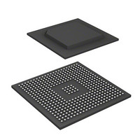
Manufacturer Part Number
R8A77850BDBGV#RD0Z
Description
IC SUPERH MPU ROMLESS 436BGA
Manufacturer
Renesas Electronics America
Series
SuperH® SH7780r
Datasheet
1.R8A77850AADBGV.pdf
(1694 pages)
Specifications of R8A77850BDBGV#RD0Z
Core Processor
SH-4A
Core Size
32-Bit
Speed
600MHz
Connectivity
Audio Codec, MMC, Serial Sound, SCI, SIO, SPI, SSI
Peripherals
DMA, POR, WDT
Number Of I /o
108
Program Memory Type
ROMless
Ram Size
8K x 8
Voltage - Supply (vcc/vdd)
1 V ~ 1.2 V
Oscillator Type
External
Operating Temperature
-40°C ~ 85°C
Package / Case
436-BGA
Lead Free Status / RoHS Status
Lead free / RoHS Compliant
Eeprom Size
-
Program Memory Size
-
Data Converters
-
Available stocks
Company
Part Number
Manufacturer
Quantity
Price


19.4.15 Double Buffer Control
The double buffer control of the display unit (DU) includes two types of functions, which are a
manual display change mode in which display switching is all controlled by software, and an auto
display change mode to realize blinking.
In the case of manual display change mode, the display change is performed in frame units for
non-interlaced and interlaced sync display, and in field units for interlaced sync & video display.
In the case of auto display change mode, all switching is performed in field units.
Manual Display Change Mode: In manual display change mode, display frame switching is
controlled by software. Display switching can either be performed by software using the PnDC bit
in PnMR, or by setting the buffer 0 or buffer 1 start address in PnDSA0R and PnDSA1R indicated
by the DFBn bit in DSSR.
When making a transition from this mode to another mode, the PnDC bit should always be set to 1
first.
The following shows a control example for the manual display mode.
Auto Display Change Mode: For information on the auto display change mode, refer to section
19.4.11, Blinking.
CPU operation
Display screen
operation
VSYNC
(Non-interlaced)
Interrupt
processing
First frame
Transfer of display data for A1
A0 display
Second frame
A0 display
Interrupt
processing
VBK: VBK bit in DSSR
Rev.1.00 Jan. 10, 2008 Page 953 of 1658
Interrupt
processing
A0: Display area start address 0
A1: Display area start address 1
Display is switched by
the PnDC bit or DSAR
at the falling edge of VSYNC.
Transfer of display data for A0
Third frame
A1 display
19. Display Unit (DU)
REJ09B0261-0100
Related parts for R8A77850BDBGV#RD0Z
Image
Part Number
Description
Manufacturer
Datasheet
Request
R

Part Number:
Description:
KIT STARTER FOR M16C/29
Manufacturer:
Renesas Electronics America
Datasheet:

Part Number:
Description:
KIT STARTER FOR R8C/2D
Manufacturer:
Renesas Electronics America
Datasheet:

Part Number:
Description:
R0K33062P STARTER KIT
Manufacturer:
Renesas Electronics America
Datasheet:

Part Number:
Description:
KIT STARTER FOR R8C/23 E8A
Manufacturer:
Renesas Electronics America
Datasheet:

Part Number:
Description:
KIT STARTER FOR R8C/25
Manufacturer:
Renesas Electronics America
Datasheet:

Part Number:
Description:
KIT STARTER H8S2456 SHARPE DSPLY
Manufacturer:
Renesas Electronics America
Datasheet:

Part Number:
Description:
KIT STARTER FOR R8C38C
Manufacturer:
Renesas Electronics America
Datasheet:

Part Number:
Description:
KIT STARTER FOR R8C35C
Manufacturer:
Renesas Electronics America
Datasheet:

Part Number:
Description:
KIT STARTER FOR R8CL3AC+LCD APPS
Manufacturer:
Renesas Electronics America
Datasheet:
Part Number:
Description:
KIT STARTER FOR RX610
Manufacturer:
Renesas Electronics America
Datasheet:

Part Number:
Description:
KIT STARTER FOR R32C/118
Manufacturer:
Renesas Electronics America
Datasheet:

Part Number:
Description:
KIT DEV RSK-R8C/26-29
Manufacturer:
Renesas Electronics America
Datasheet:

Part Number:
Description:
KIT STARTER FOR SH7124
Manufacturer:
Renesas Electronics America
Datasheet:

Part Number:
Description:
KIT STARTER FOR H8SX/1622
Manufacturer:
Renesas Electronics America
Datasheet:

Part Number:
Description:
KIT DEV FOR SH7203
Manufacturer:
Renesas Electronics America
Datasheet: