R8A77850BDBGV#RD0Z Renesas Electronics America, R8A77850BDBGV#RD0Z Datasheet - Page 65
R8A77850BDBGV#RD0Z
Manufacturer Part Number
R8A77850BDBGV#RD0Z
Description
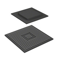
IC SUPERH MPU ROMLESS 436BGA
Manufacturer
Renesas Electronics America
Series
SuperH® SH7780r
Datasheet
1.R8A77850AADBGV.pdf
(1694 pages)
Specifications of R8A77850BDBGV#RD0Z
Core Processor
SH-4A
Core Size
32-Bit
Speed
600MHz
Connectivity
Audio Codec, MMC, Serial Sound, SCI, SIO, SPI, SSI
Peripherals
DMA, POR, WDT
Number Of I /o
108
Program Memory Type
ROMless
Ram Size
8K x 8
Voltage - Supply (vcc/vdd)
1 V ~ 1.2 V
Oscillator Type
External
Operating Temperature
-40°C ~ 85°C
Package / Case
436-BGA
Lead Free Status / RoHS Status
Lead free / RoHS Compliant
Eeprom Size
-
Program Memory Size
-
Data Converters
-
Available stocks
Company
Part Number
Manufacturer
Quantity
Price


2.2.4
(1)
Bit
31
30
29
28
Initial value:
Initial value:
Status Register (SR)
R/W:
R/W:
BIt:
BIt:
Control Registers
Bit Name
—
MD
RB
BL
R/W
FD
31
15
R
0
0
R/W
MD
30
14
R
1
0
R/W
RB
29
13
R
Initial
Value
0
1
1
1
1
0
R/W
28
BL
12
R
0
1
R/W
R
R/W
R/W
R/W
27
11
R
R
0
0
26
10
R
R
0
0
Description
Reserved
For details on reading/writing this bit, see General
Precautions on Handling of Product.
Processing Mode
Selects the processing mode.
0: User mode (Some instructions cannot be executed
1: Privileged mode
This bit is set to 1 by an exception or interrupt.
Privileged Mode General Register Bank Specification
Bit
0: R0_BANK0 to R7_BANK0 are accessed as general
1: R0_BANK1 to R7_BANK1 are accessed as general
This bit is set to 1 by an exception or interrupt.
Exception/Interrupt Block Bit
This bit is set to 1 by a reset, a general exception, or an
interrupt.
While this bit is set to 1, an interrupt request is masked.
In this case, this processor enters the reset state when
a general exception other than a user break occurs.
R/W
25
M
and some resources cannot be accessed.)
registers R0 to R7 and R0_BANK1 to R7_BANK1 can
be accessed using LDC/STC instructions
registers R0 to R7 and R0_BANK0–R7_BANK0 can
be accessed using LDC/STC instructions
R
0
9
0
R/W
24
Q
R
0
8
0
R/W
23
R
0
7
1
R/W
22
R
0
6
1
Rev.1.00 Jan. 10, 2008 Page 33 of 1658
IMASK
R/W
21
R
0
5
1
R/W
20
R
0
4
1
19
2. Programming Model
R
R
0
3
0
REJ09B0261-0100
18
R
R
0
2
0
R/W
17
R
S
0
1
0
R/W
16
R
T
0
0
0
Related parts for R8A77850BDBGV#RD0Z
Image
Part Number
Description
Manufacturer
Datasheet
Request
R

Part Number:
Description:
KIT STARTER FOR M16C/29
Manufacturer:
Renesas Electronics America
Datasheet:

Part Number:
Description:
KIT STARTER FOR R8C/2D
Manufacturer:
Renesas Electronics America
Datasheet:

Part Number:
Description:
R0K33062P STARTER KIT
Manufacturer:
Renesas Electronics America
Datasheet:

Part Number:
Description:
KIT STARTER FOR R8C/23 E8A
Manufacturer:
Renesas Electronics America
Datasheet:

Part Number:
Description:
KIT STARTER FOR R8C/25
Manufacturer:
Renesas Electronics America
Datasheet:

Part Number:
Description:
KIT STARTER H8S2456 SHARPE DSPLY
Manufacturer:
Renesas Electronics America
Datasheet:

Part Number:
Description:
KIT STARTER FOR R8C38C
Manufacturer:
Renesas Electronics America
Datasheet:

Part Number:
Description:
KIT STARTER FOR R8C35C
Manufacturer:
Renesas Electronics America
Datasheet:

Part Number:
Description:
KIT STARTER FOR R8CL3AC+LCD APPS
Manufacturer:
Renesas Electronics America
Datasheet:
Part Number:
Description:
KIT STARTER FOR RX610
Manufacturer:
Renesas Electronics America
Datasheet:

Part Number:
Description:
KIT STARTER FOR R32C/118
Manufacturer:
Renesas Electronics America
Datasheet:

Part Number:
Description:
KIT DEV RSK-R8C/26-29
Manufacturer:
Renesas Electronics America
Datasheet:

Part Number:
Description:
KIT STARTER FOR SH7124
Manufacturer:
Renesas Electronics America
Datasheet:

Part Number:
Description:
KIT STARTER FOR H8SX/1622
Manufacturer:
Renesas Electronics America
Datasheet:

Part Number:
Description:
KIT DEV FOR SH7203
Manufacturer:
Renesas Electronics America
Datasheet: