R8A77850ADBGV#RD0Z Renesas Electronics America, R8A77850ADBGV#RD0Z Datasheet - Page 713
R8A77850ADBGV#RD0Z
Manufacturer Part Number
R8A77850ADBGV#RD0Z
Description
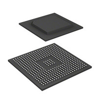
IC SUPERH MPU ROMLESS 436-BGA
Manufacturer
Renesas Electronics America
Series
SuperH® SH7780r
Datasheet
1.R8A77850AADBGV.pdf
(1694 pages)
Specifications of R8A77850ADBGV#RD0Z
Core Processor
SH-4A
Core Size
32-Bit
Speed
600MHz
Connectivity
Audio Codec, MMC, Serial Sound, SCI, SIO, SPI, SSI
Peripherals
DMA, POR, WDT
Number Of I /o
108
Program Memory Type
ROMless
Ram Size
8K x 8
Voltage - Supply (vcc/vdd)
1 V ~ 1.2 V
Oscillator Type
External
Operating Temperature
-40°C ~ 85°C
Package / Case
436-BGA
Lead Free Status / RoHS Status
Lead free / RoHS Compliant
Eeprom Size
-
Program Memory Size
-
Data Converters
-
Available stocks
Company
Part Number
Manufacturer
Quantity
Price

Part Number:
R8A77850ADBGV#RD0ZR8A77850ADBGV
Manufacturer:
Renesas Electronics America
Quantity:
10 000


14.3.7
CHCR are 32-bit readable/writable registers that control the DMA transfer mode.
Bit
31
30
29, 28
Initial value:
Initial value:
R/W:
R/W:
Note: * R/(W): To clear the flag, 0 can be written to.
Bit:
Bit:
DMA Channel Control Registers 0 to 11 (CHCR0 to CHCR11)
Bit Name
⎯
LCKN
⎯
R/W
31
15
R
0
0
DM[1:0]
LCKN
R/W
R/W
30
14
1
0
R/W
29
13
Initial
Value
0
1
All 0
R
0
0
SM[1:0]
R/W
28
12
R
0
0
R/W
R/W
27
11
R/W
R
R/W
R
0
0
RPT[2:0]
R/W
R/W
26
10
0
0
RS[3:0]
Descriptions
Reserved
This bit is always read as 0. The write value should
always be 0.
Bus Lock Signal Disable
Specifies whether the bus lock signal output is enabled
or disabled during a read instruction for the
SuperHyway bus. This bit is valid in cycle steal mode.
Clear this bit to 0 in burst mode.
If the bus lock signal is disabled, the bus request from
the bus master other than the DMAC can be accepted.
This can improve the bus usage efficiency in the
system.
For channels 0 to 5, this bit can be set to 0 or 1.
For channels 6 to 11, do not clear this bit to 0. The write
value should always be 1.
0: Bus lock signal output enabled
1: Bus lock signal output disabled
Reserved
These bits are always read as 0. The write value should
always be 0.
R/W
R/W
25
0
9
0
R/W
24
R
0
8
0
R/W
R/W
DO
23
DL
0
0
7
14. Direct Memory Access Controller (DMAC)
R/W
Rev.1.00 Jan. 10, 2008 Page 681 of 1658
R/W
DS
RL
22
6
0
0
R/W
TB
21
R
0
5
0
R/W R/(W)* R/W
R/W
TS2
20
0
4
0
TS[1:0]
R/W
HE
19
0
3
0
REJ09B0261-0100
R/W R/(W)*
HIE
18
IE
0
2
0
R/W
AM
17
TE
0
1
0
R/W
R/W
DE
16
AL
0
0
0
Related parts for R8A77850ADBGV#RD0Z
Image
Part Number
Description
Manufacturer
Datasheet
Request
R

Part Number:
Description:
KIT STARTER FOR M16C/29
Manufacturer:
Renesas Electronics America
Datasheet:

Part Number:
Description:
KIT STARTER FOR R8C/2D
Manufacturer:
Renesas Electronics America
Datasheet:

Part Number:
Description:
R0K33062P STARTER KIT
Manufacturer:
Renesas Electronics America
Datasheet:

Part Number:
Description:
KIT STARTER FOR R8C/23 E8A
Manufacturer:
Renesas Electronics America
Datasheet:

Part Number:
Description:
KIT STARTER FOR R8C/25
Manufacturer:
Renesas Electronics America
Datasheet:

Part Number:
Description:
KIT STARTER H8S2456 SHARPE DSPLY
Manufacturer:
Renesas Electronics America
Datasheet:

Part Number:
Description:
KIT STARTER FOR R8C38C
Manufacturer:
Renesas Electronics America
Datasheet:

Part Number:
Description:
KIT STARTER FOR R8C35C
Manufacturer:
Renesas Electronics America
Datasheet:

Part Number:
Description:
KIT STARTER FOR R8CL3AC+LCD APPS
Manufacturer:
Renesas Electronics America
Datasheet:
Part Number:
Description:
KIT STARTER FOR RX610
Manufacturer:
Renesas Electronics America
Datasheet:

Part Number:
Description:
KIT STARTER FOR R32C/118
Manufacturer:
Renesas Electronics America
Datasheet:

Part Number:
Description:
KIT DEV RSK-R8C/26-29
Manufacturer:
Renesas Electronics America
Datasheet:

Part Number:
Description:
KIT STARTER FOR SH7124
Manufacturer:
Renesas Electronics America
Datasheet:

Part Number:
Description:
KIT STARTER FOR H8SX/1622
Manufacturer:
Renesas Electronics America
Datasheet:

Part Number:
Description:
KIT DEV FOR SH7203
Manufacturer:
Renesas Electronics America
Datasheet: