HD6417034AFI20 Renesas Electronics America, HD6417034AFI20 Datasheet - Page 450
HD6417034AFI20
Manufacturer Part Number
HD6417034AFI20
Description
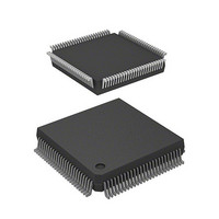
IC SUPERH MPU ROMLESS 112QFP
Manufacturer
Renesas Electronics America
Series
SuperH® SH7030r
Datasheet
1.HD6417034AFI20.pdf
(689 pages)
Specifications of HD6417034AFI20
Core Processor
SH-1
Core Size
32-Bit
Speed
20MHz
Connectivity
EBI/EMI, SCI
Peripherals
DMA, POR, PWM, WDT
Number Of I /o
32
Program Memory Type
ROMless
Ram Size
4K x 8
Voltage - Supply (vcc/vdd)
4.5 V ~ 5.5 V
Data Converters
A/D 8x10b
Oscillator Type
Internal
Operating Temperature
-20°C ~ 75°C
Package / Case
112-QFP
Lead Free Status / RoHS Status
Contains lead / RoHS non-compliant
Eeprom Size
-
Program Memory Size
-
Available stocks
Company
Part Number
Manufacturer
Quantity
Price
Company:

Part Number:
HD6417034AFI20
Manufacturer:
Renesas Electronics America
Quantity:
10 000
Company:
Part Number:
HD6417034AFI20V
Manufacturer:
Renesas Electronics America
Quantity:
10 000


Section 14 A/D Converter
14.4.2
Scan mode can be used to monitor analog inputs on one or more channels. When the ADST bit in
ADCSR is set to 1 by software or an external trigger input, A/D conversion starts with the first
channel (AN0 when CH2 = 0, AN4 when CH2 = 1) in the group.
If the scan group includes more than one channel, conversion of the second channel (AN1 or
AN5) begins as soon as conversion of the first channel ends.
Conversion of the selected channels continues cyclically until the ADST bit is cleared to 0. The
conversion results are stored in the data registers corresponding to the selected channels.
Before changing a mode or analog input channels, clear the ADST bit in ADCSR to 0 to stop A/D
conversion in order to prevent malfunctions. Setting the ADST bit to 1 after changing the mode or
channel selects the first channel and starts A/D conversion again (changing the mode or channel
and setting the ADST bit can be performed simultaneously).
The following is an example of the A/D conversion process in scan mode when three channels in
group 0 are selected (AN0, AN1, and AN2). See figure 14.4 for the timing.
1. The program selects scan mode (SCAN = 1), scan group 0 (CH2 = 0), and analog input
2. The A/D converter samples the input at the first channel (AN0), converts the voltage level to a
3. Then it does the same for the third channel (AN2).
4. After all selected channels (AN0–AN2) have been converted, the A/D converter sets the ADF
5. Steps 2–4 are repeated cyclically as long as the ADST bit remains set at 1.
Rev. 7.00 Jan 31, 2006 page 422 of 658
REJ09B0272-0700
channels AN0–AN2 (CH1 = 1, CH2 = CH0 = 0), then sets the ADST bit to 1 to start A/D
conversion.
digital value, and transfers the result to register ADDRA. Next, the second channel (AN1) is
automatically selected and conversion begins.
bit to 1 and begins conversion on channel AN0 again. If the ADIE bit is set to 1, an A/D
interrupt (ADI) is requested after the A/D conversion.
To stop A/D conversion, clear the ADST bit to 0. The moment the ADST bit is set to 1 again,
A/D conversion begins with the first channel (AN0).
Scan Mode (SCAN = 1)
Related parts for HD6417034AFI20
Image
Part Number
Description
Manufacturer
Datasheet
Request
R

Part Number:
Description:
KIT STARTER FOR M16C/29
Manufacturer:
Renesas Electronics America
Datasheet:

Part Number:
Description:
KIT STARTER FOR R8C/2D
Manufacturer:
Renesas Electronics America
Datasheet:

Part Number:
Description:
R0K33062P STARTER KIT
Manufacturer:
Renesas Electronics America
Datasheet:

Part Number:
Description:
KIT STARTER FOR R8C/23 E8A
Manufacturer:
Renesas Electronics America
Datasheet:

Part Number:
Description:
KIT STARTER FOR R8C/25
Manufacturer:
Renesas Electronics America
Datasheet:

Part Number:
Description:
KIT STARTER H8S2456 SHARPE DSPLY
Manufacturer:
Renesas Electronics America
Datasheet:

Part Number:
Description:
KIT STARTER FOR R8C38C
Manufacturer:
Renesas Electronics America
Datasheet:

Part Number:
Description:
KIT STARTER FOR R8C35C
Manufacturer:
Renesas Electronics America
Datasheet:

Part Number:
Description:
KIT STARTER FOR R8CL3AC+LCD APPS
Manufacturer:
Renesas Electronics America
Datasheet:
Part Number:
Description:
KIT STARTER FOR RX610
Manufacturer:
Renesas Electronics America
Datasheet:

Part Number:
Description:
KIT STARTER FOR R32C/118
Manufacturer:
Renesas Electronics America
Datasheet:

Part Number:
Description:
KIT DEV RSK-R8C/26-29
Manufacturer:
Renesas Electronics America
Datasheet:

Part Number:
Description:
KIT STARTER FOR SH7124
Manufacturer:
Renesas Electronics America
Datasheet:

Part Number:
Description:
KIT STARTER FOR H8SX/1622
Manufacturer:
Renesas Electronics America
Datasheet:

Part Number:
Description:
KIT DEV FOR SH7203
Manufacturer:
Renesas Electronics America
Datasheet: