HD6417034AFI20 Renesas Electronics America, HD6417034AFI20 Datasheet - Page 346
HD6417034AFI20
Manufacturer Part Number
HD6417034AFI20
Description
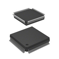
IC SUPERH MPU ROMLESS 112QFP
Manufacturer
Renesas Electronics America
Series
SuperH® SH7030r
Datasheet
1.HD6417034AFI20.pdf
(689 pages)
Specifications of HD6417034AFI20
Core Processor
SH-1
Core Size
32-Bit
Speed
20MHz
Connectivity
EBI/EMI, SCI
Peripherals
DMA, POR, PWM, WDT
Number Of I /o
32
Program Memory Type
ROMless
Ram Size
4K x 8
Voltage - Supply (vcc/vdd)
4.5 V ~ 5.5 V
Data Converters
A/D 8x10b
Oscillator Type
Internal
Operating Temperature
-20°C ~ 75°C
Package / Case
112-QFP
Lead Free Status / RoHS Status
Contains lead / RoHS non-compliant
Eeprom Size
-
Program Memory Size
-
Available stocks
Company
Part Number
Manufacturer
Quantity
Price
Company:

Part Number:
HD6417034AFI20
Manufacturer:
Renesas Electronics America
Quantity:
10 000
Company:
Part Number:
HD6417034AFI20V
Manufacturer:
Renesas Electronics America
Quantity:
10 000


Section 11 Programmable Timing Pattern Controller (TPC)
11.2.2
The port B data register (PBDR) is a 16-bit read/write register that stores output data for groups 0–
3 when TPC output is used. For details of PBDR, see section 16, I/O Ports.
Note: * Bits set to TPC output by NDERA or NDERB are read-only.
Note: * Bits set to TPC output by NDERA or NDERB are read-only.
11.2.3
NDRA is an eight-bit read/write register that stores the next output data for TPC output groups 1
and 0 (TP7–TP0). When used for TPC output, the contents of NDRA are transferred to the
corresponding PBDR bits when the ITU compare match specified in the TPC output control
register, TPCR, occurs.
The address of NDRA differs depending on whether TPCR settings select the same trigger or
different triggers for TPC output groups 1 and 0. NDRA is initialized to H'00 by a reset. It is not
initialized in standby mode.
Same Trigger for TPC Output Groups 1 and 0: If TPC output groups 1 and 0 are triggered by
the same compare match, the address of NDRA is H'FFFFF5. The upper 4 bits become group 1
and the lower 4 bits become group 0. Address H'5FFFFF7 in such cases consists entirely of
reserved bits. These bits cannot be modified and are always read as 1.
Address H'5FFFFF5
Bits 7–4—Next Data 7–4 (NDR7–NDR4): NDR7–NDR4 store the next output data for TPC
output group 1.
Rev. 7.00 Jan 31, 2006 page 318 of 658
REJ09B0272-0700
Bit
Initial value
Read/Write
Bit
Initial value
Read/Write
Port B Data Register (PBDR)
Next Data Register A (NDRA)
PB15DR PB14DR PB13DR PB12DR PB11DR PB10DR PB9DR
PB7DR
R/(W) *
R/(W) *
15
0
7
0
PB6DR
R/(W) *
R/(W) *
14
0
6
0
PB5DR
R/(W) *
R/(W) *
13
0
5
0
PB4DR
R/(W) *
R/(W) *
12
0
4
0
PB3DR
R/(W) *
R/(W) *
11
0
3
0
PB2DR
R/(W) *
R/(W) *
10
0
2
0
PB1DR
R/(W) *
R/(W) *
9
0
1
0
PB8DR
PB0DR
R/(W) *
R/(W) *
8
0
0
0
Related parts for HD6417034AFI20
Image
Part Number
Description
Manufacturer
Datasheet
Request
R

Part Number:
Description:
KIT STARTER FOR M16C/29
Manufacturer:
Renesas Electronics America
Datasheet:

Part Number:
Description:
KIT STARTER FOR R8C/2D
Manufacturer:
Renesas Electronics America
Datasheet:

Part Number:
Description:
R0K33062P STARTER KIT
Manufacturer:
Renesas Electronics America
Datasheet:

Part Number:
Description:
KIT STARTER FOR R8C/23 E8A
Manufacturer:
Renesas Electronics America
Datasheet:

Part Number:
Description:
KIT STARTER FOR R8C/25
Manufacturer:
Renesas Electronics America
Datasheet:

Part Number:
Description:
KIT STARTER H8S2456 SHARPE DSPLY
Manufacturer:
Renesas Electronics America
Datasheet:

Part Number:
Description:
KIT STARTER FOR R8C38C
Manufacturer:
Renesas Electronics America
Datasheet:

Part Number:
Description:
KIT STARTER FOR R8C35C
Manufacturer:
Renesas Electronics America
Datasheet:

Part Number:
Description:
KIT STARTER FOR R8CL3AC+LCD APPS
Manufacturer:
Renesas Electronics America
Datasheet:
Part Number:
Description:
KIT STARTER FOR RX610
Manufacturer:
Renesas Electronics America
Datasheet:

Part Number:
Description:
KIT STARTER FOR R32C/118
Manufacturer:
Renesas Electronics America
Datasheet:

Part Number:
Description:
KIT DEV RSK-R8C/26-29
Manufacturer:
Renesas Electronics America
Datasheet:

Part Number:
Description:
KIT STARTER FOR SH7124
Manufacturer:
Renesas Electronics America
Datasheet:

Part Number:
Description:
KIT STARTER FOR H8SX/1622
Manufacturer:
Renesas Electronics America
Datasheet:

Part Number:
Description:
KIT DEV FOR SH7203
Manufacturer:
Renesas Electronics America
Datasheet: