HD6417034AFI20 Renesas Electronics America, HD6417034AFI20 Datasheet - Page 300
HD6417034AFI20
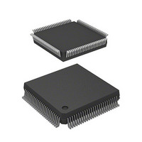
Manufacturer Part Number
HD6417034AFI20
Description
IC SUPERH MPU ROMLESS 112QFP
Manufacturer
Renesas Electronics America
Series
SuperH® SH7030r
Datasheet
1.HD6417034AFI20.pdf
(689 pages)
Specifications of HD6417034AFI20
Core Processor
SH-1
Core Size
32-Bit
Speed
20MHz
Connectivity
EBI/EMI, SCI
Peripherals
DMA, POR, PWM, WDT
Number Of I /o
32
Program Memory Type
ROMless
Ram Size
4K x 8
Voltage - Supply (vcc/vdd)
4.5 V ~ 5.5 V
Data Converters
A/D 8x10b
Oscillator Type
Internal
Operating Temperature
-20°C ~ 75°C
Package / Case
112-QFP
Lead Free Status / RoHS Status
Contains lead / RoHS non-compliant
Eeprom Size
-
Program Memory Size
-
Available stocks
Company
Part Number
Manufacturer
Quantity
Price
Company:

Part Number:
HD6417034AFI20
Manufacturer:
Renesas Electronics America
Quantity:
10 000
Company:
Part Number:
HD6417034AFI20V
Manufacturer:
Renesas Electronics America
Quantity:
10 000


Section 10 16-Bit Integrated Timer Pulse Unit (ITU)
10.4.5
In reset-synchronized PWM mode, three pairs of complementary positive and negative PWM
waveforms that share a common wave turning point can be obtained using channels 3 and 4. When
set for reset-synchronized PWM mode, the TIOCA3, TIOCB3, TIOCA4, TOCXA4, TIOCB4, and
TOCXB4 pins become PWM output pins and TCNT3 becomes an up-counter. Table 10.12 shows
the PWM output pins used and table 10.13 shows the settings of the registers used.
Table 10.12 Output Pins for Reset-Synchronized PWM Mode
Channel
3
4
Table 10.13 Register Settings for Reset-Synchronized PWM Mode
Procedure for Selecting Reset-Synchronized PWM Mode (figure 10.31):
1. Clear the STR3 bit in TSTR to halt TCNT3. Reset-synchronized PWM mode must be set while
2. Set bits TPSC2-TPSC0 in TCR to select the counter clock source for channel 3. If an external
3. Set bits CCLR1 and CCLR0 in TCR3 to select GRA3 as a counter clear source.
4. Set bits CMD1 and CMD0 in TFCR to select reset-synchronized PWM mode. TIOCA3,
5. Reset TCNT3 (to H'0000). TCNT4 need not be set.
Rev. 7.00 Jan 31, 2006 page 272 of 658
REJ09B0272-0700
Register Setting
TCNT3
TCNT4
GRA3
GRB3
GRA4
GRB4
TCNT3 is halted.
clock source is selected, select the external clock edge with bits CKEG1 and CKEG0 in TCR.
TIOCB3, TIOCA4, TIOCB4, TOCXA4, and TOCXB4 become PWM output pins.
Reset-Synchronized PWM Mode
Initial setting of H'0000
Not used (functions independently)
Sets count cycle for TCNT3
Sets the turning point for PWM waveform output by the TIOCA3 and TIOCB3 pins
Sets the turning point for PWM waveform output by the TIOCA4 and TOCXA4 pins
Sets the turning point for PWM waveform output by the TIOCB4 and TOCXB4 pins
Output Pin
TIOCA3
TIOCB3
TIOCA4
TOCXA4
TIOCB4
TOCXB4
Description
PWM output 1
PWM output 1' (negative-phase waveform of PWM output 1)
PWM output 2
PWM output 2' (negative-phase waveform of PWM output 2)
PWM output 3
PWM output 3' (negative-phase waveform of PWM output 3)
Related parts for HD6417034AFI20
Image
Part Number
Description
Manufacturer
Datasheet
Request
R

Part Number:
Description:
KIT STARTER FOR M16C/29
Manufacturer:
Renesas Electronics America
Datasheet:

Part Number:
Description:
KIT STARTER FOR R8C/2D
Manufacturer:
Renesas Electronics America
Datasheet:

Part Number:
Description:
R0K33062P STARTER KIT
Manufacturer:
Renesas Electronics America
Datasheet:

Part Number:
Description:
KIT STARTER FOR R8C/23 E8A
Manufacturer:
Renesas Electronics America
Datasheet:

Part Number:
Description:
KIT STARTER FOR R8C/25
Manufacturer:
Renesas Electronics America
Datasheet:

Part Number:
Description:
KIT STARTER H8S2456 SHARPE DSPLY
Manufacturer:
Renesas Electronics America
Datasheet:

Part Number:
Description:
KIT STARTER FOR R8C38C
Manufacturer:
Renesas Electronics America
Datasheet:

Part Number:
Description:
KIT STARTER FOR R8C35C
Manufacturer:
Renesas Electronics America
Datasheet:

Part Number:
Description:
KIT STARTER FOR R8CL3AC+LCD APPS
Manufacturer:
Renesas Electronics America
Datasheet:
Part Number:
Description:
KIT STARTER FOR RX610
Manufacturer:
Renesas Electronics America
Datasheet:

Part Number:
Description:
KIT STARTER FOR R32C/118
Manufacturer:
Renesas Electronics America
Datasheet:

Part Number:
Description:
KIT DEV RSK-R8C/26-29
Manufacturer:
Renesas Electronics America
Datasheet:

Part Number:
Description:
KIT STARTER FOR SH7124
Manufacturer:
Renesas Electronics America
Datasheet:

Part Number:
Description:
KIT STARTER FOR H8SX/1622
Manufacturer:
Renesas Electronics America
Datasheet:

Part Number:
Description:
KIT DEV FOR SH7203
Manufacturer:
Renesas Electronics America
Datasheet: