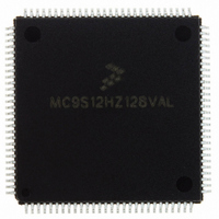
MC9S12HZ128VAL Freescale Semiconductor, MC9S12HZ128VAL Datasheet - Page 586

MC9S12HZ128VAL
Manufacturer Part Number
MC9S12HZ128VAL
Description
IC MCU 16BIT 2K FLASH 112-LQFP
Manufacturer
Freescale Semiconductor
Series
HCS12r
Datasheet
1.MC9S12HZ128CAL.pdf
(692 pages)
Specifications of MC9S12HZ128VAL
Core Processor
HCS12
Core Size
16-Bit
Speed
25MHz
Connectivity
CAN, EBI/EMI, I²C, SCI, SPI
Peripherals
LCD, Motor control PWM, POR, PWM, WDT
Number Of I /o
85
Program Memory Size
128KB (128K x 8)
Program Memory Type
FLASH
Eeprom Size
2K x 8
Ram Size
6K x 8
Voltage - Supply (vcc/vdd)
2.35 V ~ 5.5 V
Data Converters
A/D 16x10b
Oscillator Type
Internal
Operating Temperature
-40°C ~ 105°C
Package / Case
112-LQFP
Processor Series
S12H
Core
HCS12
Data Bus Width
16 bit
Data Ram Size
6 KB
Interface Type
I2C/SCI/SPI
Maximum Clock Frequency
50 MHz
Number Of Programmable I/os
85
Number Of Timers
8
Maximum Operating Temperature
+ 105 C
Mounting Style
SMD/SMT
3rd Party Development Tools
EWHCS12
Minimum Operating Temperature
- 40 C
On-chip Adc
16-ch x 10-bit
Lead Free Status / RoHS Status
Lead free / RoHS Compliant
Available stocks
Company
Part Number
Manufacturer
Quantity
Price
Company:
Part Number:
MC9S12HZ128VAL
Manufacturer:
Freescale Semiconductor
Quantity:
10 000
Part Number:
MC9S12HZ128VAL
Manufacturer:
FREESCALE
Quantity:
20 000
- Current page: 586 of 692
- Download datasheet (4Mb)
Chapter 21 Multiplexed External Bus Interface (MEBIV3)
21.3.2.7
Read: Anytime when register is in the map
Write: Anytime when register is in the map
Data direction register E is associated with port E. For bits in port E that are configured as general-purpose
I/O lines, DDRE determines the primary direction of each of these pins. A 1 causes the associated bit to
be an output and a 0 causes the associated bit to be an input. Port E bit 1 (associated with IRQ) and bit 0
(associated with XIRQ) cannot be configured as outputs. Port E, bits 1 and 0, can be read regardless of
whether the alternate interrupt function is enabled. The value in a DDR bit also affects the source of data
for reads of the corresponding PORTE register. If the DDR bit is 0 (input) the buffered pin input state is
read. If the DDR bit is 1 (output) the associated port data register bit state is read.
This register is not in the on-chip memory map in expanded and special peripheral modes. Therefore, these
accesses will be echoed externally. Also, it is not in the map in expanded modes while the EME control bit
is set.
586
Reset
DDRE
Field
7:2
W
R
Bit 7
Data Direction Port E
0 Configure the corresponding I/O pin as an input
1 Configure the corresponding I/O pin as an output
Note: It is unwise to write PORTE and DDRE as a word access. If you are changing port E pins from inputs to
Data Direction Register E (DDRE)
0
7
outputs, the data may have extra transitions during the write. It is best to initialize PORTE before enabling
as outputs.
= Unimplemented or Reserved
6
0
6
Figure 21-11. Data Direction Register E (DDRE)
Table 21-5. DDRE Field Descriptions
MC9S12HZ256 Data Sheet, Rev. 2.05
5
0
5
4
0
4
Description
3
0
3
Bit 2
0
2
Freescale Semiconductor
0
0
1
0
0
0
Related parts for MC9S12HZ128VAL
Image
Part Number
Description
Manufacturer
Datasheet
Request
R
Part Number:
Description:
Manufacturer:
Freescale Semiconductor, Inc
Datasheet:
Part Number:
Description:
Manufacturer:
Freescale Semiconductor, Inc
Datasheet:
Part Number:
Description:
Manufacturer:
Freescale Semiconductor, Inc
Datasheet:
Part Number:
Description:
Manufacturer:
Freescale Semiconductor, Inc
Datasheet:
Part Number:
Description:
Manufacturer:
Freescale Semiconductor, Inc
Datasheet:
Part Number:
Description:
Manufacturer:
Freescale Semiconductor, Inc
Datasheet:
Part Number:
Description:
Manufacturer:
Freescale Semiconductor, Inc
Datasheet:
Part Number:
Description:
Manufacturer:
Freescale Semiconductor, Inc
Datasheet:
Part Number:
Description:
Manufacturer:
Freescale Semiconductor, Inc
Datasheet:
Part Number:
Description:
Manufacturer:
Freescale Semiconductor, Inc
Datasheet:
Part Number:
Description:
Manufacturer:
Freescale Semiconductor, Inc
Datasheet:
Part Number:
Description:
Manufacturer:
Freescale Semiconductor, Inc
Datasheet:
Part Number:
Description:
Manufacturer:
Freescale Semiconductor, Inc
Datasheet:
Part Number:
Description:
Manufacturer:
Freescale Semiconductor, Inc
Datasheet:
Part Number:
Description:
Manufacturer:
Freescale Semiconductor, Inc
Datasheet:


