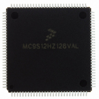
MC9S12HZ128VAL Freescale Semiconductor, MC9S12HZ128VAL Datasheet - Page 47

MC9S12HZ128VAL
Manufacturer Part Number
MC9S12HZ128VAL
Description
IC MCU 16BIT 2K FLASH 112-LQFP
Manufacturer
Freescale Semiconductor
Series
HCS12r
Datasheet
1.MC9S12HZ128CAL.pdf
(692 pages)
Specifications of MC9S12HZ128VAL
Core Processor
HCS12
Core Size
16-Bit
Speed
25MHz
Connectivity
CAN, EBI/EMI, I²C, SCI, SPI
Peripherals
LCD, Motor control PWM, POR, PWM, WDT
Number Of I /o
85
Program Memory Size
128KB (128K x 8)
Program Memory Type
FLASH
Eeprom Size
2K x 8
Ram Size
6K x 8
Voltage - Supply (vcc/vdd)
2.35 V ~ 5.5 V
Data Converters
A/D 16x10b
Oscillator Type
Internal
Operating Temperature
-40°C ~ 105°C
Package / Case
112-LQFP
Processor Series
S12H
Core
HCS12
Data Bus Width
16 bit
Data Ram Size
6 KB
Interface Type
I2C/SCI/SPI
Maximum Clock Frequency
50 MHz
Number Of Programmable I/os
85
Number Of Timers
8
Maximum Operating Temperature
+ 105 C
Mounting Style
SMD/SMT
3rd Party Development Tools
EWHCS12
Minimum Operating Temperature
- 40 C
On-chip Adc
16-ch x 10-bit
Lead Free Status / RoHS Status
Lead free / RoHS Compliant
Available stocks
Company
Part Number
Manufacturer
Quantity
Price
Company:
Part Number:
MC9S12HZ128VAL
Manufacturer:
Freescale Semiconductor
Quantity:
10 000
Part Number:
MC9S12HZ128VAL
Manufacturer:
FREESCALE
Quantity:
20 000
- Current page: 47 of 692
- Download datasheet (4Mb)
1.7
Eight possible modes determine the operating configuration of the MC9S12HZ256. Each mode has an
associated default memory map and external bus configuration.
Three low power modes exist for the device.
The operating mode out of reset is determined by the states of the MODC, MODB, and MODA pins during
reset
mode and provide limited mode switching during operation. The states of the MODC, MODB, and MODA
pins are latched into these bits on the rising edge of the reset signal.
There are two basic types of operating modes:
A system development and debug feature, background debug mode (BDM), is available in all modes. In
special single-chip mode, BDM is active immediately after reset.
Some aspects of port E are not mode dependent. Bit 1 of port E is a general-purpose input or the IRQ
interrupt input. IRQ can be enabled by bits in the CPU’s condition codes register but it is inhibited at reset
so this pin is initially configured as a simple input with a pull-up. Bit 0 of port E is a general-purpose input
or the XIRQ interrupt input. XIRQ can be enabled by bits in the CPU’s condition codes register but it is
inhibited at reset so this pin is initially configured as a simple input with a pull-up. The ESTR bit in the
EBICTL register is set to one by reset in any user mode. This assures that the reset vector can be fetched
even if it is located in an external slow memory device. The PE6/MODB/IPIPE1 and PE5/MODA/IPIPE0
pins act as pull-down select inputs during reset and high-impedance select inputs after reset.
The following paragraphs discuss the default bus setup and describe which aspects of the bus can be
changed after reset on a per mode basis.
Freescale Semiconductor
1. Normal modes: Some registers and bits are protected against accidental changes.
2. Special modes: Allow greater access to protected control registers and bits for special purposes such
MODC
X
(Table
0
0
0
1
1
1
as testing.
Modes of Operation
1-10). The MODC, MODB, and MODA bits in the MODE register show the current operating
MODB
0
0
1
1
0
0
1
MODA
0
1
0
1
0
1
1
Special Single Chip, BDM allowed and ACTIVE. BDM is allowed in all other modes
but a serial command is required to make BDM active.
Emulation Expanded Narrow, BDM allowed
Reserved for factory test
Emulation Expanded Wide, BDM allowed
Normal Single Chip, BDM allowed
Normal Expanded Narrow, BDM allowed
Normal Expanded Wide, BDM allowed
MC9S12HZ256 Data Sheet, Rev. 2.05
Table 1-10. Mode Selection
Mode Description
Chapter 1 MC9S12HZ256 Device Overview
47
Related parts for MC9S12HZ128VAL
Image
Part Number
Description
Manufacturer
Datasheet
Request
R
Part Number:
Description:
Manufacturer:
Freescale Semiconductor, Inc
Datasheet:
Part Number:
Description:
Manufacturer:
Freescale Semiconductor, Inc
Datasheet:
Part Number:
Description:
Manufacturer:
Freescale Semiconductor, Inc
Datasheet:
Part Number:
Description:
Manufacturer:
Freescale Semiconductor, Inc
Datasheet:
Part Number:
Description:
Manufacturer:
Freescale Semiconductor, Inc
Datasheet:
Part Number:
Description:
Manufacturer:
Freescale Semiconductor, Inc
Datasheet:
Part Number:
Description:
Manufacturer:
Freescale Semiconductor, Inc
Datasheet:
Part Number:
Description:
Manufacturer:
Freescale Semiconductor, Inc
Datasheet:
Part Number:
Description:
Manufacturer:
Freescale Semiconductor, Inc
Datasheet:
Part Number:
Description:
Manufacturer:
Freescale Semiconductor, Inc
Datasheet:
Part Number:
Description:
Manufacturer:
Freescale Semiconductor, Inc
Datasheet:
Part Number:
Description:
Manufacturer:
Freescale Semiconductor, Inc
Datasheet:
Part Number:
Description:
Manufacturer:
Freescale Semiconductor, Inc
Datasheet:
Part Number:
Description:
Manufacturer:
Freescale Semiconductor, Inc
Datasheet:
Part Number:
Description:
Manufacturer:
Freescale Semiconductor, Inc
Datasheet:


