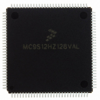
MC9S12HZ128VAL Freescale Semiconductor, MC9S12HZ128VAL Datasheet - Page 41

MC9S12HZ128VAL
Manufacturer Part Number
MC9S12HZ128VAL
Description
IC MCU 16BIT 2K FLASH 112-LQFP
Manufacturer
Freescale Semiconductor
Series
HCS12r
Datasheet
1.MC9S12HZ128CAL.pdf
(692 pages)
Specifications of MC9S12HZ128VAL
Core Processor
HCS12
Core Size
16-Bit
Speed
25MHz
Connectivity
CAN, EBI/EMI, I²C, SCI, SPI
Peripherals
LCD, Motor control PWM, POR, PWM, WDT
Number Of I /o
85
Program Memory Size
128KB (128K x 8)
Program Memory Type
FLASH
Eeprom Size
2K x 8
Ram Size
6K x 8
Voltage - Supply (vcc/vdd)
2.35 V ~ 5.5 V
Data Converters
A/D 16x10b
Oscillator Type
Internal
Operating Temperature
-40°C ~ 105°C
Package / Case
112-LQFP
Processor Series
S12H
Core
HCS12
Data Bus Width
16 bit
Data Ram Size
6 KB
Interface Type
I2C/SCI/SPI
Maximum Clock Frequency
50 MHz
Number Of Programmable I/os
85
Number Of Timers
8
Maximum Operating Temperature
+ 105 C
Mounting Style
SMD/SMT
3rd Party Development Tools
EWHCS12
Minimum Operating Temperature
- 40 C
On-chip Adc
16-ch x 10-bit
Lead Free Status / RoHS Status
Lead free / RoHS Compliant
Available stocks
Company
Part Number
Manufacturer
Quantity
Price
Company:
Part Number:
MC9S12HZ128VAL
Manufacturer:
Freescale Semiconductor
Quantity:
10 000
Part Number:
MC9S12HZ128VAL
Manufacturer:
FREESCALE
Quantity:
20 000
- Current page: 41 of 692
- Download datasheet (4Mb)
1.5.6.12
PK7 is a general-purpose input or output pin. It can be configured as frontplane segment driver output
FP23 of the LCD module.
During MCU expanded modes of operation, this pin is used as the emulation chip select output (ECS).
During MCU expanded modes of operation, this pin is used to enable the Flash EEPROM memory in the
memory map (ROMCTL). At the rising edge of RESET, the state of this pin is latched to the ROMON bit.
For all other modes the reset state of the ROMON bit is as follows:
1.5.6.13
PK3–PK0 are general-purpose input or output pins. They can be configured as backplane segment driver
outputs BP3–BP0 of the LCD module. In MCU expanded modes of operation, these pins provide the
expanded address XADDR[17:14] for the external bus.
1.5.6.14
PL7–PL4 are general-purpose input or output pins. They can be configured as frontplane segment driver
outputs FP31–FP28 of the LCD module or analog inputs for the analog-to-digital converter.
1.5.6.15
PL3–PL0 are general-purpose input or output pins. They can be configured as frontplane segment driver
outputs FP19–FP16 of the LCD module or analog inputs for the analog-to-digital converter.
1.5.6.16
PM5 is a general-purpose input or output pin. It can be configured as the transmit pin TXCAN1 of the
scalable controller area network controller 1 (CAN1)
1.5.6.17
PM4 is a general-purpose input or output pin. It can be configured as the receive pin RXCAN1 of the
scalable controller area network controller 1 (CAN1)
1.5.6.18
PM3 is a general-purpose input or output pin. It can be configured as the transmit pin TXCAN0 of the
scalable controller area network controller 0 (CAN0)
Freescale Semiconductor
Special single: ROMCTL = 1
Normal single: ROMCTL = 1
Emulation expanded wide: ROMCTL = 0
Emulation expanded narrow: ROMCTL = 0
Special test: ROMCTL = 0
Peripheral test: ROMCTL = 1
PK7 / FP23 / ECS / ROMCTL — Port K I/O Pin 7
PK[3:0] / BP[3:0] / XADDR[17:14] — Port K I/O Pins [3:0]
PL[7:4] / FP[31:28] / AN[15:12] — Port L I/O Pins [7:4]
PL[3:0] / FP[19:16] / AN[11:8] — Port L I/O Pins [3:0]
PM5 / TXCAN1 — Port M I/O Pin 5
PM4 / RXCAN1 — Port M I/O Pin 4
PM3 / TXCAN0 — Port M I/O Pin 3
MC9S12HZ256 Data Sheet, Rev. 2.05
Chapter 1 MC9S12HZ256 Device Overview
41
Related parts for MC9S12HZ128VAL
Image
Part Number
Description
Manufacturer
Datasheet
Request
R
Part Number:
Description:
Manufacturer:
Freescale Semiconductor, Inc
Datasheet:
Part Number:
Description:
Manufacturer:
Freescale Semiconductor, Inc
Datasheet:
Part Number:
Description:
Manufacturer:
Freescale Semiconductor, Inc
Datasheet:
Part Number:
Description:
Manufacturer:
Freescale Semiconductor, Inc
Datasheet:
Part Number:
Description:
Manufacturer:
Freescale Semiconductor, Inc
Datasheet:
Part Number:
Description:
Manufacturer:
Freescale Semiconductor, Inc
Datasheet:
Part Number:
Description:
Manufacturer:
Freescale Semiconductor, Inc
Datasheet:
Part Number:
Description:
Manufacturer:
Freescale Semiconductor, Inc
Datasheet:
Part Number:
Description:
Manufacturer:
Freescale Semiconductor, Inc
Datasheet:
Part Number:
Description:
Manufacturer:
Freescale Semiconductor, Inc
Datasheet:
Part Number:
Description:
Manufacturer:
Freescale Semiconductor, Inc
Datasheet:
Part Number:
Description:
Manufacturer:
Freescale Semiconductor, Inc
Datasheet:
Part Number:
Description:
Manufacturer:
Freescale Semiconductor, Inc
Datasheet:
Part Number:
Description:
Manufacturer:
Freescale Semiconductor, Inc
Datasheet:
Part Number:
Description:
Manufacturer:
Freescale Semiconductor, Inc
Datasheet:


