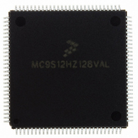
MC9S12HZ128VAL Freescale Semiconductor, MC9S12HZ128VAL Datasheet - Page 138

MC9S12HZ128VAL
Manufacturer Part Number
MC9S12HZ128VAL
Description
IC MCU 16BIT 2K FLASH 112-LQFP
Manufacturer
Freescale Semiconductor
Series
HCS12r
Datasheet
1.MC9S12HZ128CAL.pdf
(692 pages)
Specifications of MC9S12HZ128VAL
Core Processor
HCS12
Core Size
16-Bit
Speed
25MHz
Connectivity
CAN, EBI/EMI, I²C, SCI, SPI
Peripherals
LCD, Motor control PWM, POR, PWM, WDT
Number Of I /o
85
Program Memory Size
128KB (128K x 8)
Program Memory Type
FLASH
Eeprom Size
2K x 8
Ram Size
6K x 8
Voltage - Supply (vcc/vdd)
2.35 V ~ 5.5 V
Data Converters
A/D 16x10b
Oscillator Type
Internal
Operating Temperature
-40°C ~ 105°C
Package / Case
112-LQFP
Processor Series
S12H
Core
HCS12
Data Bus Width
16 bit
Data Ram Size
6 KB
Interface Type
I2C/SCI/SPI
Maximum Clock Frequency
50 MHz
Number Of Programmable I/os
85
Number Of Timers
8
Maximum Operating Temperature
+ 105 C
Mounting Style
SMD/SMT
3rd Party Development Tools
EWHCS12
Minimum Operating Temperature
- 40 C
On-chip Adc
16-ch x 10-bit
Lead Free Status / RoHS Status
Lead free / RoHS Compliant
Available stocks
Company
Part Number
Manufacturer
Quantity
Price
Company:
Part Number:
MC9S12HZ128VAL
Manufacturer:
Freescale Semiconductor
Quantity:
10 000
Part Number:
MC9S12HZ128VAL
Manufacturer:
FREESCALE
Quantity:
20 000
- Current page: 138 of 692
- Download datasheet (4Mb)
Chapter 4 Port Integration Module (PIM9HZ256V2)
4.3.4
Port P is associated with the Pulse Width Modulator (PWM), serial communication interface (SCI1) and
Inter-IC bus (IIC) modules. Each pin is assigned to these modules according to the following priority:
PWM > SCI1/IIC > general-purpose I/O.
When a PWM channel is enabled, the corresponding pin becomes a PWM output with the exception of
PP[5] which can be PWM input or output. Refer to the PWM block description chapter for information on
enabling and disabling the PWM channels.
When the IIC bus is enabled, the PP[5:4] pins become SCL and SDA respectively as long as the
corresponding PWM channels are disabled. Refer to the IIC block description chapter for information on
enabling and disabling the IIC bus.
When the SCI1 receiver and transmitter are enabled, the PP[2] and PP[0] pins become RXD1 and TXD1
respectively as long as the corresponding PWM channels are disabled. Refer to the SCI block description
chapter for information on enabling and disabling the SCI receiver and transmitter.
During reset, port P pins are configured as high-impedance inputs.
4.3.4.1
Read: Anytime. Write: Anytime.
If the associated data direction bit (DDRPx) is set to 1 (output), a read returns the value of the I/O register
bit. If the associated data direction bit (DDRPx) is set to 0 (input), a read returns the value of the pin.
The PWM function takes precedence over the general-purpose I/O function if the associated PWM
channel is enabled. The PWM channels 4-0 are outputs if the respective channels are enabled. PWM
channel 5 can be an output, or an input if the shutdown feature is enabled.
The IIC function takes precedence over the general-purpose I/O function if the IIC bus is enabled and the
corresponding PWM channels remain disabled. The SDA and SCL pins are bidirectional with outputs
configured as open-drain.
If enabled, the SCI1 transmitter takes precedence over the general-purpose I/O function, and the
corresponding TXD1 pin is configured as an output. If enabled, the SCI1 receiver takes precedence over
the general-purpose I/O function, and the corresponding RXD1 pin is configured as an input.
138
SCI1/IIC:
PWM:
Reset
W
R
Port P
Port P I/O Register (PTP)
0
0
7
= Reserved or Unimplemented
0
0
6
Figure 4-23. Port P I/O Register (PTP)
PWM5
PTP5
MC9S12HZ256 Data Sheet, Rev. 2.05
SCL
0
5
PWM4
PTP4
SDA
0
4
PWM3
PTP3
0
3
PWM2
PTP2
RXD1
0
2
Freescale Semiconductor
PWM1
PTP1
0
1
PWM0
PTP0
TXD1
0
0
Related parts for MC9S12HZ128VAL
Image
Part Number
Description
Manufacturer
Datasheet
Request
R
Part Number:
Description:
Manufacturer:
Freescale Semiconductor, Inc
Datasheet:
Part Number:
Description:
Manufacturer:
Freescale Semiconductor, Inc
Datasheet:
Part Number:
Description:
Manufacturer:
Freescale Semiconductor, Inc
Datasheet:
Part Number:
Description:
Manufacturer:
Freescale Semiconductor, Inc
Datasheet:
Part Number:
Description:
Manufacturer:
Freescale Semiconductor, Inc
Datasheet:
Part Number:
Description:
Manufacturer:
Freescale Semiconductor, Inc
Datasheet:
Part Number:
Description:
Manufacturer:
Freescale Semiconductor, Inc
Datasheet:
Part Number:
Description:
Manufacturer:
Freescale Semiconductor, Inc
Datasheet:
Part Number:
Description:
Manufacturer:
Freescale Semiconductor, Inc
Datasheet:
Part Number:
Description:
Manufacturer:
Freescale Semiconductor, Inc
Datasheet:
Part Number:
Description:
Manufacturer:
Freescale Semiconductor, Inc
Datasheet:
Part Number:
Description:
Manufacturer:
Freescale Semiconductor, Inc
Datasheet:
Part Number:
Description:
Manufacturer:
Freescale Semiconductor, Inc
Datasheet:
Part Number:
Description:
Manufacturer:
Freescale Semiconductor, Inc
Datasheet:
Part Number:
Description:
Manufacturer:
Freescale Semiconductor, Inc
Datasheet:


