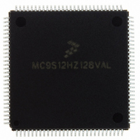
MC9S12HZ128VAL Freescale Semiconductor, MC9S12HZ128VAL Datasheet - Page 223

MC9S12HZ128VAL
Manufacturer Part Number
MC9S12HZ128VAL
Description
IC MCU 16BIT 2K FLASH 112-LQFP
Manufacturer
Freescale Semiconductor
Series
HCS12r
Datasheet
1.MC9S12HZ128CAL.pdf
(692 pages)
Specifications of MC9S12HZ128VAL
Core Processor
HCS12
Core Size
16-Bit
Speed
25MHz
Connectivity
CAN, EBI/EMI, I²C, SCI, SPI
Peripherals
LCD, Motor control PWM, POR, PWM, WDT
Number Of I /o
85
Program Memory Size
128KB (128K x 8)
Program Memory Type
FLASH
Eeprom Size
2K x 8
Ram Size
6K x 8
Voltage - Supply (vcc/vdd)
2.35 V ~ 5.5 V
Data Converters
A/D 16x10b
Oscillator Type
Internal
Operating Temperature
-40°C ~ 105°C
Package / Case
112-LQFP
Processor Series
S12H
Core
HCS12
Data Bus Width
16 bit
Data Ram Size
6 KB
Interface Type
I2C/SCI/SPI
Maximum Clock Frequency
50 MHz
Number Of Programmable I/os
85
Number Of Timers
8
Maximum Operating Temperature
+ 105 C
Mounting Style
SMD/SMT
3rd Party Development Tools
EWHCS12
Minimum Operating Temperature
- 40 C
On-chip Adc
16-ch x 10-bit
Lead Free Status / RoHS Status
Lead free / RoHS Compliant
Available stocks
Company
Part Number
Manufacturer
Quantity
Price
Company:
Part Number:
MC9S12HZ128VAL
Manufacturer:
Freescale Semiconductor
Quantity:
10 000
Part Number:
MC9S12HZ128VAL
Manufacturer:
FREESCALE
Quantity:
20 000
- Current page: 223 of 692
- Download datasheet (4Mb)
Freescale Semiconductor
C[D:A}
Field
3:0
SRES8
Analog Input Channel Select Code — These bits select the analog input channel(s) whose signals are
sampled and converted to digital codes.
channels.
In the case of single channel conversions (MULT = 0), this selection code specified the channel to be examined.
In the case of multiple channel conversions (MULT = 1), this selection code represents the first channel to be
examined in the conversion sequence. Subsequent channels are determined by incrementing the channel
selection code or wrapping around to AN0 (after converting the channel defined by the Wrap Around Channel
Select Bits WRAP[3:0] in ATDCTL0). In case starting with a channel number higher than the one defined by
WRAP[3:0] the first wrap around will be AN15 to AN0.
1
1
1
0
0
0
V
RH
V
Input Signal
5.120 Volts
RL
= 5.12 Volts
Table 7-16. Left Justified, Signed and Unsigned ATD Output Codes.
5.100
5.080
2.580
2.560
2.540
0.020
0.000
= 0 Volts
Table 7-14. ATDCTL5 Field Descriptions (continued)
DJM
0
0
1
0
0
1
Table 7-15. Available Result Data Formats.
MC9S12HZ256 Data Sheet, Rev. 2.05
8-Bit Codes
Signed
DSGN
7F
7F
7E
FF
01
00
81
80
X
X
0
1
0
1
Table 7-17
Description
8-Bit Codes
Unsigned
lists the coding used to select the various analog input
10-bit / left justified / unsigned — bits 15:6
10-bit / right justified / unsigned — bits 9:0
8-bit / left justified / unsigned — bits 15:8
8-bit / right justified / unsigned — bits 7:0
10-bit / left justified / signed -— bits 15:6
FF
FF
FE
81
80
7F
01
00
8-bit / left justified / signed — bits 15:8
Description and Bus Bit Mapping
Chapter 7 Analog-to-Digital Converter (ATD10B16CV4)
Result Data Formats
10-Bit Codes
Signed
7FC0
7E00
FF00
7F00
0100
0000
8100
8000
10-Bit Codes
Unsigned
FFC0
FE00
FF00
7F00
8100
8000
0100
0000
223
Related parts for MC9S12HZ128VAL
Image
Part Number
Description
Manufacturer
Datasheet
Request
R
Part Number:
Description:
Manufacturer:
Freescale Semiconductor, Inc
Datasheet:
Part Number:
Description:
Manufacturer:
Freescale Semiconductor, Inc
Datasheet:
Part Number:
Description:
Manufacturer:
Freescale Semiconductor, Inc
Datasheet:
Part Number:
Description:
Manufacturer:
Freescale Semiconductor, Inc
Datasheet:
Part Number:
Description:
Manufacturer:
Freescale Semiconductor, Inc
Datasheet:
Part Number:
Description:
Manufacturer:
Freescale Semiconductor, Inc
Datasheet:
Part Number:
Description:
Manufacturer:
Freescale Semiconductor, Inc
Datasheet:
Part Number:
Description:
Manufacturer:
Freescale Semiconductor, Inc
Datasheet:
Part Number:
Description:
Manufacturer:
Freescale Semiconductor, Inc
Datasheet:
Part Number:
Description:
Manufacturer:
Freescale Semiconductor, Inc
Datasheet:
Part Number:
Description:
Manufacturer:
Freescale Semiconductor, Inc
Datasheet:
Part Number:
Description:
Manufacturer:
Freescale Semiconductor, Inc
Datasheet:
Part Number:
Description:
Manufacturer:
Freescale Semiconductor, Inc
Datasheet:
Part Number:
Description:
Manufacturer:
Freescale Semiconductor, Inc
Datasheet:
Part Number:
Description:
Manufacturer:
Freescale Semiconductor, Inc
Datasheet:


