EVAL-ADUC832QSZ Analog Devices Inc, EVAL-ADUC832QSZ Datasheet - Page 53
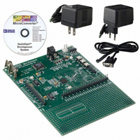
EVAL-ADUC832QSZ
Manufacturer Part Number
EVAL-ADUC832QSZ
Description
KIT DEV FOR ADUC832 QUICK START
Manufacturer
Analog Devices Inc
Series
QuickStart™ Kitr
Type
MCUr
Specifications of EVAL-ADUC832QSZ
Contents
Evaluation Board, Cable, Power Supply, Software and Documentation
Lead Free Status / RoHS Status
Lead free / RoHS Compliant
For Use With/related Products
ADuC832
Lead Free Status / RoHS Status
Compliant, Lead free / RoHS Compliant
Other names
EVAL-ADUC832QS
EVAL-ADUC832QS
EVAL-ADUC832QS


TIMER/COUNTER 0 AND 1 OPERATING MODES
The following paragraphs describe the operating modes for
Timer/Counters 0 and 1. Unless otherwise noted, it should be
assumed that these modes of operation are the same for Timer 0
as for Timer 1.
Mode 0 (13-Bit Timer/Counter)
Mode 0 configures an 8-bit timer/counter with a divide-by-32
prescaler. Figure 45 shows Mode 0 operation.
In this mode, the timer register is configured as a 13-bit register.
As the count rolls over from all 1s to all 0s, it sets the timer
overflow flag TF0. The overflow flag, TF0, can then be used to
request an interrupt. The counted input is enabled to the timer
when TR0 = 1 and either Gate = 0 or INT0 = 1. Setting Gate = 1
allows the timer to be controlled by external input INT0 to facili-
tate pulsewidth measurements. TR0 is a control bit in the special
function register TCON; Gate is in TMOD. The 13-bit register
consists of all eight bits of TH0 and the lower five bits of TL0.
The upper three bits of TL0 are indeterminate and should be
ignored. Setting the run flag (TR0) does not clear the registers.
Mode 1 (16-Bit Timer/Counter)
Mode 1 is the same as Mode 0, except that the timer register is
running with all 16 bits. Mode 1 is shown in Figure 46.
REV. 0
P3.4/T0
P3.2/INT0
*CORE CLK IS DEFINED BY THE CD BITS IN PLLCON
P3.4/T0
P3.2/INT0
*CORE CLK IS DEFINED BY THE CD BITS IN PLLCON
CORE
CORE
CLK*
CLK*
GATE
GATE
Figure 45. Timer/Counter 0, Mode 0
Figure 46. Timer/Counter 0, Mode 1
12
12
TR0
TR0
C/T = 0
C/T = 1
C/T = 0
C/T = 1
CONTROL
CONTROL
(5 BITS)
(8 BITS)
TL0
TL0
(8 BITS)
(8 BITS)
TH0
TH0
TF0
TF0
INTERRUPT
INTERRUPT
–53–
Mode 2 (8-Bit Timer/Counter with Autoreload)
Mode 2 configures the timer register as an 8-bit counter (TL0)
with automatic reload, as shown in Figure 47. Overflow from TL0
not only sets TF0, but also reloads TL0 with the contents of TH0,
which is preset by software. The reload leaves TH0 unchanged.
Mode 3 (Two 8-Bit Timer/Counters)
Mode 3 has different effects on Timer 0 and Timer 1. Timer 1
in Mode 3 simply holds its count. The effect is the same as setting
TR1 = 0. Timer 0 in Mode 3 establishes TL0 and TH0 as two
separate counters. This configuration is shown in Figure 48. TL0
uses the Timer 0 control bits: C/T, Gate, TR0, INT0, and TF0.
TH0 is locked into a timer function (counting machine cycles)
and takes over the use of TR1 and TF1 from Timer 1. Thus,
TH0 now controls the Timer 1 interrupt. Mode 3 is provided
for applications requiring an extra 8-bit timer or counter.
When Timer 0 is in Mode 3, Timer 1 can be turned on and
off by switching it out of and into its own Mode 3, or can still be
used by the serial interface as a baud rate generator. In fact, it
can be used in any application not requiring an interrupt from
Timer 1 itself.
P3.2/INTO
P3.4/T0
*CORE CLK IS DEFINED BY THE CD BITS IN PLLCON
P3.2/INT0
P3.4/T0
*CORE CLK IS DEFINED BY THE CD BITS IN PLLCON
CORE
CLK*
CLK/12
CORE
GATE
CLK*
CORE
GATE
TR1
Figure 47. Timer/Counter 0, Mode 2
Figure 48. Timer/Counter 0, Mode 3
12
12
TR0
TR0
C/ T = 0
C/ T = 1
C/T = 0
C/T = 1
CORE
CLK/12
CONTROL
CONTROL
RELOAD
(8 BITS)
(8 BITS)
(8 BITS)
(8 BITS)
TH0
TL0
TH0
TL0
ADuC832
TF0
TF0
TF1
INTERRUPT
INTERRUPT
INTERRUPT
Related parts for EVAL-ADUC832QSZ
Image
Part Number
Description
Manufacturer
Datasheet
Request
R


Part Number:
Description:
BOARD EVAL FOR SI270X-A
Manufacturer:
Silicon Laboratories Inc
Datasheet:

Part Number:
Description:
BUCK CONV REF DESIGN KIT IP1201
Manufacturer:
International Rectifier
Datasheet:
Part Number:
Description:
BOARD DEMO SYNC DUAL BUCK CNVTER
Manufacturer:
International Rectifier
Datasheet:
Part Number:
Description:
BOARD DEMO SYNC BUCK CONVETER
Manufacturer:
International Rectifier
Datasheet:

Part Number:
Description:
EVALBOARD/EB Omnidirectional microphone - Analog
Manufacturer:
Analog Devices
Datasheet:
Part Number:
Description:
EVALBOARD/EB Omnidirectional microphone - Analog
Manufacturer:
Analog Devices
Datasheet:


Part Number:
Description:
BOARD EVAL LED DRIVER LT3756
Manufacturer:
Linear Technology
Datasheet:

Part Number:
Description:
BOARD EVAL FOR AD7741/7742
Manufacturer:
Analog Devices Inc
Datasheet:

Part Number:
Description:
±1.7g Dual-Axis IMEMS Accelerometer Evaluation Board
Manufacturer:
Analog Devices Inc
Datasheet:

Part Number:
Description:
IC MULTIPLIER ANALOG 8-SOIC T/R
Manufacturer:
Analog Devices Inc
Datasheet:

Part Number:
Description:
IC ANALOG MULTIPLIER 8-DIP
Manufacturer:
Analog Devices Inc
Datasheet:
Part Number:
Description:
IC ANALOG MULTIPLIER 8-SOIC
Manufacturer:
Analog Devices Inc
Datasheet:
Part Number:
Description:
IC ANALOG MULTIPLIER 8-DIP
Manufacturer:
Analog Devices Inc
Datasheet: