EVAL-ADUC832QSZ Analog Devices Inc, EVAL-ADUC832QSZ Datasheet - Page 50
EVAL-ADUC832QSZ
Manufacturer Part Number
EVAL-ADUC832QSZ
Description
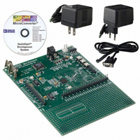
KIT DEV FOR ADUC832 QUICK START
Manufacturer
Analog Devices Inc
Series
QuickStart™ Kitr
Type
MCUr
Specifications of EVAL-ADUC832QSZ
Contents
Evaluation Board, Cable, Power Supply, Software and Documentation
Lead Free Status / RoHS Status
Lead free / RoHS Compliant
For Use With/related Products
ADuC832
Lead Free Status / RoHS Status
Compliant, Lead free / RoHS Compliant
Other names
EVAL-ADUC832QS
EVAL-ADUC832QS
EVAL-ADUC832QS


ADuC832
MISO is shared with P3.3 and as such has the same configuration
as that shown in Figure 40.
*These instructions read the port byte (all 8 bits), modify the addressed bit and
then write the new byte back to the latch.
Figure 43. SDATA/MOSI Pin I/O Functional Equivalent
in SPI Mode
Figure 44. SDATA/MOSI Pin I/O Functional Equivalent
in I
BITS
SFR
SPE = 0 (I
MDO
MDE
I2CM
Figure 42. SCLOCK Pin I/O Functional Equivalent
in I
MDI
(MASTER/SLAVE)
2
HARDWARE SPI
C Mode
HARDWARE I
(SLAVE ONLY)
SPE = 0 (I
HARDWARE I
2
(SLAVE ONLY)
BITS
MCO
I2CM
C Mode
SFR
2
C ENABLE)
SPE = 1 (SPI ENABLE)
2
C ENABLE)
REJECTION FILTER
2
REJECTION FILTER
C
2
C
50ns GLITCH
50ns GLITCH
Q1
Q3
DV
DD
DV
Q1
(OFF)
Q3
DD
Q2 (OFF)
Q4 (OFF)
Q2
Q4
DV
Q1
(OFF)
Q3
SCLOCK
DD
PIN
SDATA/
Q2
Q4
MOSI
PIN
SDATA/
MOSI
PIN
–50–
Read-Modify-Write Instructions
Some 8051 instructions that read a port read the latch while
others read the pin. The instructions that read the latch rather
than the pins are the ones that read a value, possibly change it,
and then rewrite it to the latch. These are called “read-modify-
write” instructions. Listed below are the read-modify-write
instructions. When the destination operand is a port, or a port
bit, these instructions read the latch rather than the pin.
The reason that read-modify-write instructions are directed to
the latch rather than the pin is to avoid a possible misinterpreta-
tion of the voltage level of a pin. For example, a port pin might
be used to drive the base of a transistor. When a 1 is written to
the bit, the transistor is turned on. If the CPU then reads the
same port bit at the pin rather than the latch, it will read the
base voltage of the transistor and interpret it as a logic 0. Reading
the latch rather than the pin will return the correct value of 1.
ANL
ORL
XRL
JBC
CPL
INC
DEC
DJNZ
MOV PX.Y, C
CLR PX.Y
SETB PX.Y
*
*
*
(Complement bit, e.g., CPL P3.0)
(Decrement, e.g., DEC P2)
(Decrement and jump if not zero, e.g., DJNZ
(Logical AND, e.g., ANL P1, A)
(Logical OR, e.g., ORL P2, A)
(Logical EX-OR, e.g., XRL P3, A)
(Jump if bit = 1 and clear bit, e.g., JBC P1.1,
LABEL)
(increment, e.g., INC P2)
P3, LABEL)
(Move carry to Bit Y of Port X)
(Clear Bit Y of Port X)
(Set Bit Y of Port X)
REV. 0
Related parts for EVAL-ADUC832QSZ
Image
Part Number
Description
Manufacturer
Datasheet
Request
R


Part Number:
Description:
BOARD EVAL FOR SI270X-A
Manufacturer:
Silicon Laboratories Inc
Datasheet:

Part Number:
Description:
BUCK CONV REF DESIGN KIT IP1201
Manufacturer:
International Rectifier
Datasheet:
Part Number:
Description:
BOARD DEMO SYNC DUAL BUCK CNVTER
Manufacturer:
International Rectifier
Datasheet:
Part Number:
Description:
BOARD DEMO SYNC BUCK CONVETER
Manufacturer:
International Rectifier
Datasheet:

Part Number:
Description:
EVALBOARD/EB Omnidirectional microphone - Analog
Manufacturer:
Analog Devices
Datasheet:
Part Number:
Description:
EVALBOARD/EB Omnidirectional microphone - Analog
Manufacturer:
Analog Devices
Datasheet:


Part Number:
Description:
BOARD EVAL LED DRIVER LT3756
Manufacturer:
Linear Technology
Datasheet:

Part Number:
Description:
BOARD EVAL FOR AD7741/7742
Manufacturer:
Analog Devices Inc
Datasheet:

Part Number:
Description:
±1.7g Dual-Axis IMEMS Accelerometer Evaluation Board
Manufacturer:
Analog Devices Inc
Datasheet:

Part Number:
Description:
IC MULTIPLIER ANALOG 8-SOIC T/R
Manufacturer:
Analog Devices Inc
Datasheet:

Part Number:
Description:
IC ANALOG MULTIPLIER 8-DIP
Manufacturer:
Analog Devices Inc
Datasheet:
Part Number:
Description:
IC ANALOG MULTIPLIER 8-SOIC
Manufacturer:
Analog Devices Inc
Datasheet:
Part Number:
Description:
IC ANALOG MULTIPLIER 8-DIP
Manufacturer:
Analog Devices Inc
Datasheet: