EVAL-ADUC832QSZ Analog Devices Inc, EVAL-ADUC832QSZ Datasheet - Page 15
EVAL-ADUC832QSZ
Manufacturer Part Number
EVAL-ADUC832QSZ
Description
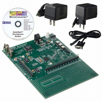
KIT DEV FOR ADUC832 QUICK START
Manufacturer
Analog Devices Inc
Series
QuickStart™ Kitr
Type
MCUr
Specifications of EVAL-ADUC832QSZ
Contents
Evaluation Board, Cable, Power Supply, Software and Documentation
Lead Free Status / RoHS Status
Lead free / RoHS Compliant
For Use With/related Products
ADuC832
Lead Free Status / RoHS Status
Compliant, Lead free / RoHS Compliant
Other names
EVAL-ADUC832QS
EVAL-ADUC832QS
EVAL-ADUC832QS


External Data Memory (External XRAM)
Just like a standard 8051 compatible core, the ADuC832 can
access external data memory using a MOVX instruction. The
MOVX instruction automatically outputs the various control
strobes required to access the data memory.
The ADuC832, however, can access up to 16 MBytes of external
data memory. This is an enhancement of the 64 kBytes external
data memory space available on a standard 8051 compatible core.
The external data memory is discussed in more detail in the
ADuC832 Hardware Design Considerations section.
Internal XRAM
2 kBytes of on-chip data memory exist on the ADuC832. This
memory, although on-chip, is also accessed via the MOVX
instruction. The 2 kBytes of internal XRAM are mapped into the
bottom 2 kBytes of the external address space if the CFG832 bit
is set. Otherwise, access to the external data memory will occur
just like a standard 8051. When using the internal XRAM,
Ports 0 and 2 are free to be used as general-purpose I/O.
SPECIAL FUNCTION REGISTERS (SFRs)
The SFR space is mapped into the upper 128 bytes of internal
data memory space and accessed by direct addressing only. It
provides an interface between the CPU and all on chip periph-
erals. A block diagram showing the programming model of the
ADuC832 via the SFR area is shown in Figure 5.
All registers, except the Program Counter (PC) and the four
general-purpose register banks, reside in the SFR area. The SFR
registers include control, configuration, and data registers that
provide an interface between the CPU and all on-chip peripherals.
REV. 0
FFFFFFH
000000H
Figure 4. Internal and External XRAM
CFG832.0 = 0
EXTERNAL
ADDRESS
MEMORY
SPACE)
SPACE
(24-BIT
DATA
FFFFFFH
0007FFH
000000H
000800H
CFG832.0 = 1
EXTERNAL
ADDRESS
2 kBYTES
MEMORY
ON-CHIP
SPACE)
SPACE
(24-BIT
DATA
XRAM
–15–
Accumulator SFR (ACC)
ACC is the Accumulator register and is used for math operations
including addition, subtraction, integer multiplication and division,
and Boolean bit manipulations. The mnemonics for accumulator-
specific instructions refer to the Accumulator as A.
B SFR (B)
The B register is used with the ACC for multiplication and divi-
sion operations. For other instructions, it can be treated as a
general-purpose scratch pad register.
Stack Pointer (SP and SPH)
The SP SFR is the stack pointer and is used to hold an internal
RAM address that is called the top of the stack. The SP register is
incremented before data is stored during PUSH and CALL execu-
tions. While the stack may reside anywhere in on-chip RAM, the
SP register is initialized to 07H after a reset. This causes the
stack to begin at location 08H.
As mentioned earlier, the ADuC832 offers an extended 11-bit
stack pointer. The three extra bits to make up the 11-bit stack
pointer are the 3 LSBs of the SPH byte located at B7H.
FLASH/EE PROGRAM
REPROGRAMMABLE
ELECTRICALLY
COMPATIBLE
NONVOLATILE
2304 BYTES
62-kBYTE
MEMORY
CORE
8051
RAM
Figure 5. Programming Model
FUNCTION
REGISTER
128-BYTE
SPECIAL
AREA
REPROGRAMMABLE
ADuC832
FLASH/EE DATA
OTHER ON-CHIP
2
ELECTRICALLY
TEMPERATURE
NONVOLATILE
PERIPHERALS
8-CHANNEL
12-BIT ADC
SERIAL I/O
MEMORY
SENSOR
4-kBYTE
12-BIT DACs
PWM
WDT
PSM
TIC
Related parts for EVAL-ADUC832QSZ
Image
Part Number
Description
Manufacturer
Datasheet
Request
R


Part Number:
Description:
BOARD EVAL FOR SI270X-A
Manufacturer:
Silicon Laboratories Inc
Datasheet:

Part Number:
Description:
BUCK CONV REF DESIGN KIT IP1201
Manufacturer:
International Rectifier
Datasheet:
Part Number:
Description:
BOARD DEMO SYNC DUAL BUCK CNVTER
Manufacturer:
International Rectifier
Datasheet:
Part Number:
Description:
BOARD DEMO SYNC BUCK CONVETER
Manufacturer:
International Rectifier
Datasheet:

Part Number:
Description:
EVALBOARD/EB Omnidirectional microphone - Analog
Manufacturer:
Analog Devices
Datasheet:
Part Number:
Description:
EVALBOARD/EB Omnidirectional microphone - Analog
Manufacturer:
Analog Devices
Datasheet:


Part Number:
Description:
BOARD EVAL LED DRIVER LT3756
Manufacturer:
Linear Technology
Datasheet:

Part Number:
Description:
BOARD EVAL FOR AD7741/7742
Manufacturer:
Analog Devices Inc
Datasheet:

Part Number:
Description:
±1.7g Dual-Axis IMEMS Accelerometer Evaluation Board
Manufacturer:
Analog Devices Inc
Datasheet:

Part Number:
Description:
IC MULTIPLIER ANALOG 8-SOIC T/R
Manufacturer:
Analog Devices Inc
Datasheet:

Part Number:
Description:
IC ANALOG MULTIPLIER 8-DIP
Manufacturer:
Analog Devices Inc
Datasheet:
Part Number:
Description:
IC ANALOG MULTIPLIER 8-SOIC
Manufacturer:
Analog Devices Inc
Datasheet:
Part Number:
Description:
IC ANALOG MULTIPLIER 8-DIP
Manufacturer:
Analog Devices Inc
Datasheet: