EVAL-ADUC832QSZ Analog Devices Inc, EVAL-ADUC832QSZ Datasheet - Page 49
EVAL-ADUC832QSZ
Manufacturer Part Number
EVAL-ADUC832QSZ
Description
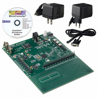
KIT DEV FOR ADUC832 QUICK START
Manufacturer
Analog Devices Inc
Series
QuickStart™ Kitr
Type
MCUr
Specifications of EVAL-ADUC832QSZ
Contents
Evaluation Board, Cable, Power Supply, Software and Documentation
Lead Free Status / RoHS Status
Lead free / RoHS Compliant
For Use With/related Products
ADuC832
Lead Free Status / RoHS Status
Compliant, Lead free / RoHS Compliant
Other names
EVAL-ADUC832QS
EVAL-ADUC832QS
EVAL-ADUC832QS


In general-purpose I/O port mode, Port 2 pins that have 1s written
to them are pulled high by the internal pull-ups (Figure 39)
and, in that state, can be used as inputs. As inputs, Port 2 pins
being pulled externally low will source current because of the
internal pull-up resistors. Port 2 pins with 0s written to them will
drive a logic low output voltage (V
sinking 1.6 mA.
P2.6 and P2.7 can also be used as PWM outputs. In the case
that they are selected as the PWM outputs via the CFG832 SFR,
the PWM outputs will overwrite anything written to P2.6 or P2.7.
Port 3
Port 3 is a bidirectional port with internal pull-ups directly
controlled via the P3 SFR. Port 3 pins that have 1s written to
them are pulled high by the internal pull-ups and, in that state,
can be used as inputs. As inputs, Port 3 pins being pulled exter-
nally low will source current because of the internal pull-ups.
Port 3 pins with 0s written to them will drive a logic low output
voltage (V
Port 3 pins also have various secondary functions described in
Table XIX. The alternate functions of Port 3 pins can only be
activated if the corresponding bit latch in the P3 SFR contains a 1.
Otherwise, the port pin is stuck at 0.
Pin
P3.0
P3.1
P3.2
P3.3
P3.4
P3.5
P3.6
P3.7
P3.3 and P3.4 can also be used as PWM outputs. In the case
that they are selected as the PWM outputs via the CFG832 SFR,
the PWM outputs will overwrite anything written to P3.4 or P3.3.
REV. 0
TO LATCH
INTERNAL
LATCH
FROM
PORT
LATCH
WRITE
READ
READ
BUS
PIN
Q
Alternate Function
RxD (UART Input Pin)(or Serial Data I/O in Mode 0)
TxD (UART Output Pin)
(or Serial Clock Output in Mode 0)
INT0 (External Interrupt 0)
INT1 (External Interrupt 1)/PWM 1/MISO
T0 (Timer/Counter 0 External Input)
PWM External Clock/PWM 0
T1 (Timer/Counter 1 External Input)
WR (External Data Memory Write Strobe)
RD (External Data Memory Read Strobe)
Figure 39. Internal Pull-Up Configuration
Figure 38. Port 2 Bit Latch and I/O Buffer
Table XIX. Port 3, Alternate Pin Functions
OL
) and will be capable of sinking 4 mA.
DELAY
2 CLK
LATCH
D
CL
Q
Q
ADDR
*SEE FIGURE 39 FOR
DETAILS OF INTERNAL PULL-UP
CONTROL
Q4
Q1
OL
DV
) and will be capable of
DD
Q2
DV
DD
DV
DD
Q3
DV
DV
DD
DD
INTERNAL
PULL-UP*
P2.x
PIN
Px.x
PIN
–49–
Additional Digital I/O
In addition to the port pins, the dedicated SPI/I
and SDATA/MOSI) also feature both input and output functions.
Their equivalent I/O architectures are illustrated in Figure 41
and Figure 43, respectively, for SPI operation and in Figure 42
and Figure 44 for I
Notice that in I
(Q1) is disabled, leaving only a weak pull-up (Q2) present.
By contrast, in SPI mode (SPE = 1) the strong pull-up FET
(Q1) is controlled directly by SPI hardware, giving the pin
push-pull capability.
In I
in parallel in order to provide an extra 60% or 70% of current
sinking capability. In SPI mode, however, (SPE = 1) only one of
the pull-down FETs (Q3) operates on each pin resulting in sink
capabilities identical to that of Port 0 and Port 2 pins.
On the input path of SCLOCK, notice that a Schmitt trigger
conditions the signal going to the SPI hardware to prevent false
triggers (double triggers) on slow incoming edges. For incoming
signals from the SCLOCK and SDATA pins going to I
ware, a filter conditions the signals in order to reject glitches of
up to 50 ns in duration.
Notice also that direct access to the SCLOCK and SDATA/MOSI
pins is afforded through the SFR interface in I
Therefore, if you are not using the SPI or I
use these two pins to give additional high current digital outputs.
2
INTERNAL
TO LATCH
C mode (SPE = 0), two pull-down FETs (Q3 and Q4) operate
(MASTER/SLAVE)
Figure 41. SCLOCK Pin I/O Functional Equivalent
in SPI Mode
HARDWARE SPI
LATCH
WRITE
READ
READ
BUS
PIN
Figure 40. Port 3 Bit Latch and I/O Buffer
SPE = 1 (SPI ENABLE)
2
C mode (SPE = 0), the strong pull-up FET
2
LATCH
D
CL
C operation.
Q
Q
SCHMITT
TRIGGER
ALTERNATE
ALTERNATE
FUNCTION
FUNCTION
OUTPUT
INPUT
Q1
Q3
DV
DD
DV
2
C functions, you can
DD
Q2 (OFF)
Q4 (OFF)
INTERNAL
PULL-UP*
*SEE FIGURE 39
ADuC832
FOR DETAILS OF
INTERNAL PULL-UP
2
2
C pins (SCLOCK
C master mode.
P3.x
PIN
SCLOCK
PIN
2
C hard-
Related parts for EVAL-ADUC832QSZ
Image
Part Number
Description
Manufacturer
Datasheet
Request
R


Part Number:
Description:
BOARD EVAL FOR SI270X-A
Manufacturer:
Silicon Laboratories Inc
Datasheet:

Part Number:
Description:
BUCK CONV REF DESIGN KIT IP1201
Manufacturer:
International Rectifier
Datasheet:
Part Number:
Description:
BOARD DEMO SYNC DUAL BUCK CNVTER
Manufacturer:
International Rectifier
Datasheet:
Part Number:
Description:
BOARD DEMO SYNC BUCK CONVETER
Manufacturer:
International Rectifier
Datasheet:

Part Number:
Description:
EVALBOARD/EB Omnidirectional microphone - Analog
Manufacturer:
Analog Devices
Datasheet:
Part Number:
Description:
EVALBOARD/EB Omnidirectional microphone - Analog
Manufacturer:
Analog Devices
Datasheet:


Part Number:
Description:
BOARD EVAL LED DRIVER LT3756
Manufacturer:
Linear Technology
Datasheet:

Part Number:
Description:
BOARD EVAL FOR AD7741/7742
Manufacturer:
Analog Devices Inc
Datasheet:

Part Number:
Description:
±1.7g Dual-Axis IMEMS Accelerometer Evaluation Board
Manufacturer:
Analog Devices Inc
Datasheet:

Part Number:
Description:
IC MULTIPLIER ANALOG 8-SOIC T/R
Manufacturer:
Analog Devices Inc
Datasheet:

Part Number:
Description:
IC ANALOG MULTIPLIER 8-DIP
Manufacturer:
Analog Devices Inc
Datasheet:
Part Number:
Description:
IC ANALOG MULTIPLIER 8-SOIC
Manufacturer:
Analog Devices Inc
Datasheet:
Part Number:
Description:
IC ANALOG MULTIPLIER 8-DIP
Manufacturer:
Analog Devices Inc
Datasheet: