EVAL-ADUC832QSZ Analog Devices Inc, EVAL-ADUC832QSZ Datasheet - Page 23
EVAL-ADUC832QSZ
Manufacturer Part Number
EVAL-ADUC832QSZ
Description
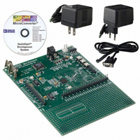
KIT DEV FOR ADUC832 QUICK START
Manufacturer
Analog Devices Inc
Series
QuickStart™ Kitr
Type
MCUr
Specifications of EVAL-ADUC832QSZ
Contents
Evaluation Board, Cable, Power Supply, Software and Documentation
Lead Free Status / RoHS Status
Lead free / RoHS Compliant
For Use With/related Products
ADuC832
Lead Free Status / RoHS Status
Compliant, Lead free / RoHS Compliant
Other names
EVAL-ADUC832QS
EVAL-ADUC832QS
EVAL-ADUC832QS


ground, no amplifier can deliver signals all the way to ground
when powered by a single supply. Therefore, if a negative
supply is available, you might consider using it to power the
front end amplifiers. If you do, however, be sure to include the
Schottky diodes shown in Figure 10 (or at least the lower of
the two diodes) to protect the analog input from undervoltage
conditions. To summarize this section, use the circuit of
Figure 10 to drive the analog input pins of the ADuC832.
Voltage Reference Connections
The on-chip 2.5 V band gap voltage reference can be used as
the reference source for the ADC and DACs. To ensure the
accuracy of the voltage reference, you must decouple the V
pin to ground with a 0.1 µF capacitor, and the C
ground with a 0.1 µF capacitor as shown in Figure 11.
If the internal voltage reference is to be used as a reference for
external circuitry, the C
buffer must be used in this case to ensure that no current is
drawn from the C
that of an internal node within the buffer block, and its voltage
is critical to ADC and DAC accuracy. On the ADuC812, V
was the recommended output for the external reference; this
can be used but it should be noted that there will be a gain error
between this reference and that of the ADC.
The ADuC832 powers up with its internal voltage reference in
the “on” state. This is available at the V
before there will be a gain error between this and that of the ADC.
The C
If an external voltage reference is preferred, it should be
connected to the V
Bit 6 of the ADCCON1 SFR must be set to 1 to switch in the
external reference voltage.
REV. 0
REF
BUFFER
output becomes available when the ADC is powered up.
Figure 11. Decoupling V
V
REF
REF
0.1 F
0.1 F
REF
C
REF
pin itself. The voltage on the C
and C
REF
output should be used. However, a
51
BUFFER
REF
pins as shown in Figure 12.
REFERENCE
BAND GAP
ADuC832
2.5V
REF
REF
and C
pin, but as noted
REF
REF
pin to
REF
pin is
REF
REF
–23–
To ensure accurate ADC operation, the voltage applied to V
must be between 1 V and AV
input signals are proportional to the power supply (such as some
strain gage applications) it may be desirable to connect the C
and V
Operation of the ADC or DACs with a reference voltage below
1 V, however, may incur loss of accuracy, eventually resulting in
missing codes or non-monotonicity. For that reason, do not use
a reference voltage less than 1 V.
To maintain compatibility with the ADuC812, the external refer-
ence may also be connected to the V
to overdrive the internal reference. Note this introduces a gain
error for the ADC that has to be calibrated out; thus the previous
method is the recommended one for most users. For this method
to work, ADCCON1.6 should be configured to use the internal
reference. The external reference will then overdrive this.
REFERENCE
REF
EXTERNAL
Figure 13. Using an External Voltage Reference
Figure 12. Using an External Voltage Reference
VOLTAGE
REFERENCE
EXTERNAL
VOLTAGE
V
DD
pins directly to AV
V
DD
0.1 F
0.1 F
V
C
REF
REF
0.1 F
0.1 F
V
C
REF
REF
51
“1” = EXTERNAL
“0” = INTERNAL
8
7
ADCCON1.6
DD
REFERENCE
DD
BAND GAP
51
BUFFER
.
. In situations where analog
2.5V
ADuC832
REF
REFERENCE
BAND GAP
pin as shown in Figure 13,
ADuC832
2.5V
BUFFER
ADuC832
REF
REF
Related parts for EVAL-ADUC832QSZ
Image
Part Number
Description
Manufacturer
Datasheet
Request
R


Part Number:
Description:
BOARD EVAL FOR SI270X-A
Manufacturer:
Silicon Laboratories Inc
Datasheet:

Part Number:
Description:
BUCK CONV REF DESIGN KIT IP1201
Manufacturer:
International Rectifier
Datasheet:
Part Number:
Description:
BOARD DEMO SYNC DUAL BUCK CNVTER
Manufacturer:
International Rectifier
Datasheet:
Part Number:
Description:
BOARD DEMO SYNC BUCK CONVETER
Manufacturer:
International Rectifier
Datasheet:

Part Number:
Description:
EVALBOARD/EB Omnidirectional microphone - Analog
Manufacturer:
Analog Devices
Datasheet:
Part Number:
Description:
EVALBOARD/EB Omnidirectional microphone - Analog
Manufacturer:
Analog Devices
Datasheet:


Part Number:
Description:
BOARD EVAL LED DRIVER LT3756
Manufacturer:
Linear Technology
Datasheet:

Part Number:
Description:
BOARD EVAL FOR AD7741/7742
Manufacturer:
Analog Devices Inc
Datasheet:

Part Number:
Description:
±1.7g Dual-Axis IMEMS Accelerometer Evaluation Board
Manufacturer:
Analog Devices Inc
Datasheet:

Part Number:
Description:
IC MULTIPLIER ANALOG 8-SOIC T/R
Manufacturer:
Analog Devices Inc
Datasheet:

Part Number:
Description:
IC ANALOG MULTIPLIER 8-DIP
Manufacturer:
Analog Devices Inc
Datasheet:
Part Number:
Description:
IC ANALOG MULTIPLIER 8-SOIC
Manufacturer:
Analog Devices Inc
Datasheet:
Part Number:
Description:
IC ANALOG MULTIPLIER 8-DIP
Manufacturer:
Analog Devices Inc
Datasheet: