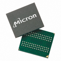
MT46H8M32LFB5-6:A TR Micron Technology Inc, MT46H8M32LFB5-6:A TR Datasheet - Page 5

MT46H8M32LFB5-6:A TR
Manufacturer Part Number
MT46H8M32LFB5-6:A TR
Description
IC DDR SDRAM 256MBIT 90VFBGA
Manufacturer
Micron Technology Inc
Type
DDR SDRAMr
Specifications of MT46H8M32LFB5-6:A TR
Format - Memory
RAM
Memory Type
Mobile DDR SDRAM
Memory Size
256M (8Mx32)
Speed
166MHz
Interface
Parallel
Voltage - Supply
1.7 V ~ 1.95 V
Operating Temperature
0°C ~ 70°C
Package / Case
90-VFBGA
Organization
8Mx32
Density
256Mb
Address Bus
14b
Access Time (max)
6.5/5ns
Maximum Clock Rate
166MHz
Operating Supply Voltage (typ)
1.8V
Package Type
VFBGA
Operating Temp Range
0C to 70C
Operating Supply Voltage (max)
1.95V
Operating Supply Voltage (min)
1.7V
Supply Current
120mA
Pin Count
90
Mounting
Surface Mount
Operating Temperature Classification
Commercial
Lead Free Status / RoHS Status
Lead free / RoHS Compliant
Other names
557-1280-2
MT46H8M32LFB5-6:A TR
MT46H8M32LFB5-6:A TR
Figure 1:
FBGA Part Marking Decoder
General Description
PDF: 09005aef82091978 / Source: 09005aef8209195b
MT46H16M16LF__2.fm - Rev. H 6/08 EN
256Mb Mobile DDR Part Numbering
Micron DDR MT46
Example Part Number: MT 46 H 16 M 1 6 L F XX-75 IT :A
Due to space limitations, FBGA-packaged components have an abbreviated part
marking that is different from the part number. For a quick conversion of an FBGA code,
see the FBGA part marking decoder at
The 256Mb Mobile DDR SDRAM is a high-speed CMOS, dynamic random-access
memory containing 268,435,456 bits. It is internally configured as a quad-bank DRAM.
On the x16 device, each of the 67,108,864-bit banks is organized as 8,192 rows by 512
columns by 16 bits. On the x32 device, each of the 67,108,864-bit banks is organized as
4,096 rows by 512 columns by 32 bits.
The 256Mb Mobile DDR SDRAM uses a double data rate architecture to achieve high-
speed operation. The double data rate architecture is essentially a 2n-prefetch architec-
ture with an interface designed to transfer two data words per clock cycle at the I/O
balls
consists of a single 2n-bit-wide, one-clock-cycle data transfer at the internal DRAM core
and two corresponding n-bit-wide, one-half-clock-cycle data transfers at the I/O balls
A bidirectional data strobe (DQS) is transmitted externally, along with data, for use in
data capture at the receiver. DQS is a strobe transmitted by the Mobile DDR SDRAM
during READs and by the memory controller during WRITEs. DQS is edge-aligned with
data for READs and center-aligned with data for WRITEs. The x16 offering has two data
strobes: one for the lower byte and one for the upper byte. The x32 offering has four data
strobes, one per byte.
V
1.8V/1.8V
DD
/V
V
.
DD
V
DD
A single read or write access for the 256Mb Mobile DDR SDRAM effectively
DD
Q
Q
/
H
Configuration
16 Meg x 16
8 Meg x 32
Mobile Configuration
Package
60-Ball VFBGA (lead-free) BF
90-Ball VFBGA (lead-free) B5
16M16LF
8M32LF
5
Package
www.micron.com/decoder.
Micron Technology, Inc., reserves the right to change products or specifications without notice.
256Mb: x16, x32 Mobile DDR SDRAM
–
-75
-10
-6
Speed
Speed Grade
t CK = 6.0ns
t CK = 7.5ns
t CK = 9.6ns
FBGA Part Marking Decoder
IT
Temp
Operating Temp
Commercial
Industrial
:A
Revision
©2005 Micron Technology, Inc. All rights reserved.
Revision
First Generation
.


