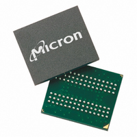
MT46H8M32LFB5-6:A TR Micron Technology Inc, MT46H8M32LFB5-6:A TR Datasheet - Page 16

MT46H8M32LFB5-6:A TR
Manufacturer Part Number
MT46H8M32LFB5-6:A TR
Description
IC DDR SDRAM 256MBIT 90VFBGA
Manufacturer
Micron Technology Inc
Type
DDR SDRAMr
Specifications of MT46H8M32LFB5-6:A TR
Format - Memory
RAM
Memory Type
Mobile DDR SDRAM
Memory Size
256M (8Mx32)
Speed
166MHz
Interface
Parallel
Voltage - Supply
1.7 V ~ 1.95 V
Operating Temperature
0°C ~ 70°C
Package / Case
90-VFBGA
Organization
8Mx32
Density
256Mb
Address Bus
14b
Access Time (max)
6.5/5ns
Maximum Clock Rate
166MHz
Operating Supply Voltage (typ)
1.8V
Package Type
VFBGA
Operating Temp Range
0C to 70C
Operating Supply Voltage (max)
1.95V
Operating Supply Voltage (min)
1.7V
Supply Current
120mA
Pin Count
90
Mounting
Surface Mount
Operating Temperature Classification
Commercial
Lead Free Status / RoHS Status
Lead free / RoHS Compliant
Other names
557-1280-2
MT46H8M32LFB5-6:A TR
MT46H8M32LFB5-6:A TR
CAS Latency
Figure 6:
PDF: 09005aef82091978 / Source: 09005aef8209195b
MT46H16M16LF__2.fm - Rev. H 6/08 EN
Standard Mode Register Definition
The CAS latency is the delay, in clock cycles, between the registration of a READ
command and the availability of the first output data. The latency can be set to two or
three clocks, as shown in Figure 7 on page 18.
For CAS latency three (CL = 3), if the READ command is registered at clock edge n, then
the data will nominally be available at (n + 2 clocks +
command is registered at clock edge n, then the data will be nominally be available at (n
+ 1 clock +
M14
0
0
1
1
M13
0
1
0
1
14
0
BA1
M12 M11 M10 M9 M8 M7 M6–M0 Operating Mode
Mode Register Definition
Standard mode register
Reserved
Extended mode register
Reserved
0
–
BA0
0
13
t
AC).
12
A12 A11
0
–
Operating Mode
11
0
–
10
A10
0
–
9
A9
0
–
A8
8
7
A7 A6 A5 A4 A3
0
M6
–
CAS Latency BT
0
0
0
0
1
1
1
1
16
6
M5
Valid
0
0
1
1
0
0
1
1
5
M4
0
1
0
1
0
1
0
1
4
M3
All other states reserved
0
1
Normal operation
3
Micron Technology, Inc., reserves the right to change products or specifications without notice.
256Mb: x16, x32 Mobile DDR SDRAM
Burst Length
M2
CAS Latency
0
0
0
0
1
1
1
1
A2 A1 A0
2
Reserved
Reserved
Reserved
Reserved
Reserved
Reserved
M1
0
0
1
1
0
0
1
1
1
Interleaved
Burst Type
Sequential
2
3
M0
0
1
0
1
0
1
0
1
0
Reserved
Reserved
Reserved
Reserved
Reserved
M3 = 0
Standard Mode Register (Mx)
t
Address Bus
2
4
8
AC). For CL = 2, if the READ
Burst Length
Reserved
Reserved
Reserved
Reserved
Reserved
M3 = 1
©2005 Micron Technology, Inc. All rights reserved.
Register Definition
2
4
8


