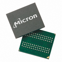
MT46H8M32LFB5-6:A TR Micron Technology Inc, MT46H8M32LFB5-6:A TR Datasheet - Page 33

MT46H8M32LFB5-6:A TR
Manufacturer Part Number
MT46H8M32LFB5-6:A TR
Description
IC DDR SDRAM 256MBIT 90VFBGA
Manufacturer
Micron Technology Inc
Type
DDR SDRAMr
Specifications of MT46H8M32LFB5-6:A TR
Format - Memory
RAM
Memory Type
Mobile DDR SDRAM
Memory Size
256M (8Mx32)
Speed
166MHz
Interface
Parallel
Voltage - Supply
1.7 V ~ 1.95 V
Operating Temperature
0°C ~ 70°C
Package / Case
90-VFBGA
Organization
8Mx32
Density
256Mb
Address Bus
14b
Access Time (max)
6.5/5ns
Maximum Clock Rate
166MHz
Operating Supply Voltage (typ)
1.8V
Package Type
VFBGA
Operating Temp Range
0C to 70C
Operating Supply Voltage (max)
1.95V
Operating Supply Voltage (min)
1.7V
Supply Current
120mA
Pin Count
90
Mounting
Surface Mount
Operating Temperature Classification
Commercial
Lead Free Status / RoHS Status
Lead free / RoHS Compliant
Other names
557-1280-2
MT46H8M32LFB5-6:A TR
MT46H8M32LFB5-6:A TR
Truncated READs
Figure 18:
PDF: 09005aef82091978 / Source: 09005aef8209195b
MT46H16M16LF__2.fm - Rev. H 6/08 EN
Command
Command
Address
Address
Terminating a READ Burst
DQS
DQS
CK#
CK#
DQ
DQ
CK
CK
Notes:
Note:
Bank a ,
Bank a ,
READ
READ
Col n
Col n
T0
T0
Data from any non-auto precharge READ burst may be truncated with a BURST TERMI-
NATE command, as shown in Figure 18. The BURST TERMINATE latency is equal to the
READ (CAS) latency; for example, the BURST TERMINATE command should be issued x
cycles after the READ command, where x equals the number of desired data element
pairs (pairs are required by the 2n-prefetch architecture).
Data from any non-auto precharge READ burst must be completed or truncated before a
subsequent WRITE command can be issued. If truncation is necessary, the BURST
TERMINATE command must be used, as shown in Figure 18. The
shown; the
[MAX] are defined in the section on WRITEs.)
A READ burst may be followed by, or truncated with, a PRECHARGE command to the
same bank provided that auto precharge was not activated. The PRECHARGE command
should be issued x cycles after the READ command, where x equals the number of
desired data element pairs (pairs are required by the n-prefetch architecture). This is
shown in Figure 20 on page 35. Following the PRECHARGE command, a subsequent
command to the same bank cannot be issued until
1. D
2. BL = 4 or 8.
3. Shown with nominal
4. BST = BURST TERMINATE command; page remains open.
Part of the row precharge time is hidden during the access of the last data elements.
OUT
CL = 2
n = data-out from column n.
t
BST
BST
DQSS (MAX) case has a longer bus idle time. (
T1
T1
CL = 3
4
4
T1n
t
D
AC,
OUT
n
T2
NOP
NOP
T2
t
DQSCK, and
33
D
n+1
T2n
OUT
T2n
D
OUT
n
T3
T3
NOP
NOP
Micron Technology, Inc., reserves the right to change products or specifications without notice.
t
256Mb: x16, x32 Mobile DDR SDRAM
Transitioning data
DQSQ.
D
n+1
T3n
OUT
t
T4
T4
NOP
NOP
RP is met.
t
DQSS [MIN] and
©2005 Micron Technology, Inc. All rights reserved.
T5
T5
NOP
Don’t Care
NOP
t
DQSS (MIN) case is
Operations
t
DQSS


