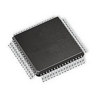
Z16FMC32AG20EG Zilog, Z16FMC32AG20EG Datasheet - Page 266

Z16FMC32AG20EG
Manufacturer Part Number
Z16FMC32AG20EG
Description
Microcontrollers (MCU) 16BIT 32K FL 2K RAM 2UART 12CH 10BIT A/D
Manufacturer
Zilog
Series
Z16FMCr
Datasheet
1.Z16FMC28AG20_EG.pdf
(341 pages)
Specifications of Z16FMC32AG20EG
Processor Series
Z16FMC
Core
ZNEO
Data Bus Width
16 bit
Program Memory Type
Flash
Program Memory Size
32 KB
Data Ram Size
2 KB
Interface Type
I2C, SPI, UART
Maximum Clock Frequency
20 MHz
Number Of Programmable I/os
46
Operating Supply Voltage
2.7 V to 3.6 V
Maximum Operating Temperature
+ 105 C
Mounting Style
SMD/SMT
Package / Case
LQFP-64
Development Tools By Supplier
Z16FMC28200KITG
Minimum Operating Temperature
- 40 C
Core Processor
ZNEO
Core Size
16-Bit
Speed
20MHz
Connectivity
I²C, IrDA, LIN, SPI, UART/USART
Peripherals
Brown-out Detect/Reset, DMA, POR, PWM, WDT
Number Of I /o
46
Eeprom Size
-
Ram Size
4K x 8
Voltage - Supply (vcc/vdd)
2.7 V ~ 3.6 V
Data Converters
A/D 12x10b
Oscillator Type
Internal
Operating Temperature
-40°C ~ 105°C
Lead Free Status / Rohs Status
Details
Available stocks
Company
Part Number
Manufacturer
Quantity
Price
Company:
Part Number:
Z16FMC32AG20EG
Manufacturer:
Zilog
Quantity:
160
- Current page: 266 of 341
- Download datasheet (21Mb)
PS028702-1210
Page Erase
Mass Erase
Flash Controller Bypass
Flash Controller Behavior using the On-Chip Debugger
4. Write a word to Program memory.
5. Repeat step 4 to program additional memory locations on the same page.
6. Write
The Flash memory is erased one page (2 KB) at a time. Page Erasing the Flash memory
sets all words in that page to the value FFFFH. The Flash Page Select register identifies
the page to be erased. While the Flash Controller executes the Page Erase operation, Flash
reads are held in wait. Interrupts that occur when the Page Erase operation is in progress
will be serviced after the Page Erase operation is complete. When the Page Erase opera-
tion is complete, the Flash Controller returns to its locked state. Only pages located in
unprotected sectors are erased.
The steps to perform a Page Erase operation are:
1. Write the page to be erased to the Flash Page Select register.
2. Write the first unlock command
3. Write the second unlock command
4. Write the Page Erase command
The Flash memory cannot be Mass Erased by user code.
The Flash Controller is bypassed and the control signals for the Flash memory brought out
to the GPIO pins. Bypassing the Flash Controller allows faster Programming algorithms
by controlling the Flash programming signals directly.
Flash Controller Bypass is recommended for large volume gang programming
applications, which do not require in-circuit programming of the Flash memory.
The following changes in behavior of the Flash Controller occur when the Flash
Controller is accessed using the On-Chip Debugger:
•
•
•
The Flash Controller does not have to be unlocked for program and erase operations.
The Flash Write Protect option bit is ignored.
The Flash Sector Protect register is ignored for programming and erase operations.
00H
to the Flash Command register to lock the Flash Controller.
P R E L I M I N A R Y
95H
73H
8CH
to the Flash Command register.
to the Flash Command register.
to the Flash Command register.
Z16FMC Series Motor Control MCUs
Product Specification
Flash Memory
244
Related parts for Z16FMC32AG20EG
Image
Part Number
Description
Manufacturer
Datasheet
Request
R

Part Number:
Description:
Microcontrollers (MCU) 16BIT 32K FL 2K RAM 2UART 12CH 10BIT A/D
Manufacturer:
Zilog
Datasheet:

Part Number:
Description:
Microcontrollers (MCU) 16BIT 128K FL 4KRAM 2UART 12CH 10BIT A/D
Manufacturer:
Zilog
Datasheet:

Part Number:
Description:
Microcontrollers (MCU) 16BIT 64K FL 4K RAM 2UART 12CH 10BIT A/D
Manufacturer:
Zilog
Datasheet:

Part Number:
Description:
Microcontrollers (MCU) 16BIT 64K FL 4K RAM 2UART 12CH 10BIT A/D
Manufacturer:
Zilog
Datasheet:

Part Number:
Description:
Microcontrollers (MCU) 16BIT 128K FL 4KRAM 2UART 12CH 10BIT A/D
Manufacturer:
Zilog

Part Number:
Description:
Communication Controllers, ZILOG INTELLIGENT PERIPHERAL CONTROLLER (ZIP)
Manufacturer:
Zilog, Inc.
Datasheet:

Part Number:
Description:
KIT DEV FOR Z8 ENCORE 16K TO 64K
Manufacturer:
Zilog
Datasheet:

Part Number:
Description:
KIT DEV Z8 ENCORE XP 28-PIN
Manufacturer:
Zilog
Datasheet:

Part Number:
Description:
DEV KIT FOR Z8 ENCORE 8K/4K
Manufacturer:
Zilog
Datasheet:

Part Number:
Description:
KIT DEV Z8 ENCORE XP 28-PIN
Manufacturer:
Zilog
Datasheet:

Part Number:
Description:
DEV KIT FOR Z8 ENCORE 4K TO 8K
Manufacturer:
Zilog
Datasheet:

Part Number:
Description:
CMOS Z8 microcontroller. ROM 16 Kbytes, RAM 256 bytes, speed 16 MHz, 32 lines I/O, 3.0V to 5.5V
Manufacturer:
Zilog, Inc.
Datasheet:

Part Number:
Description:
Low-cost microcontroller. 512 bytes ROM, 61 bytes RAM, 8 MHz
Manufacturer:
Zilog, Inc.
Datasheet:

Part Number:
Description:
Z8 4K OTP Microcontroller
Manufacturer:
Zilog, Inc.
Datasheet:


