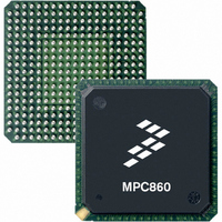
MC68MH360ZP33L Freescale Semiconductor, MC68MH360ZP33L Datasheet - Page 645

MC68MH360ZP33L
Manufacturer Part Number
MC68MH360ZP33L
Description
IC MPU 32BIT QUICC 357-PBGA
Manufacturer
Freescale Semiconductor
Specifications of MC68MH360ZP33L
Processor Type
M683xx 32-Bit
Speed
33MHz
Voltage
5V
Mounting Type
Surface Mount
Package / Case
357-PBGA
Lead Free Status / RoHS Status
Contains lead / RoHS non-compliant
Features
-
Available stocks
Company
Part Number
Manufacturer
Quantity
Price
Company:
Part Number:
MC68MH360ZP33L
Manufacturer:
FREESCALE
Quantity:
1 831
Company:
Part Number:
MC68MH360ZP33L
Manufacturer:
MOTOLOLA
Quantity:
672
Company:
Part Number:
MC68MH360ZP33L
Manufacturer:
Freescale Semiconductor
Quantity:
10 000
Part Number:
MC68MH360ZP33L
Manufacturer:
FREESCALE
Quantity:
20 000
Company:
Part Number:
MC68MH360ZP33LR2
Manufacturer:
Freescale Semiconductor
Quantity:
10 000
- Current page: 645 of 962
- Download datasheet (5Mb)
RAM values will not normally need to be accessed by user software. They should only be
modified when no SPI activity is in progress.
7.12.5.3.1 BD Table Pointer (RBASE, TBASE). The RBASE and TBASE entries define
the starting location in the dual-port RAM for the set of BDs for receive and transmit func-
tions of the SPI. This provides a great deal of flexibility in how BDs for an SPI are partitioned.
By setting the W-bit in the last BD in each BD list, the user may select how many BDs to
allocate for the transmit and receive side of the SPI. The user must initialize these entries
before enabling the SPI. Furthermore, the user should not configure BD tables of the SPI to
overlap any other serial channel’s BDs, or erratic operation will occur.
7.12.5.3.2 SPI Function Code Registers (RFCR, TFCR). The FC entry contains the value
that the user would like to appear on the function code pins (FC3–FC0), when the associ-
ated SDMA channel accesses memory. It also controls the byte-ordering convention to be
used in the transfers.
Receive Function Code Register
Bits 7–5—Reserved
MOT—Motorola
FC3–FC0—Function Code 3–0
Transmit Function Code Register
MOTOROLA
These bits should be set to zero by the user.
This bit should be set by the user to achieve normal operation. MOT must be set if the
data buffer is located in external memory and has a 16-bit wide memory port size.
These bits contain the function code value used during this SDMA channel’s memory ac-
cesses. The user should write bit FC3 with a one to identify this SDMA channel access as
a DMA-type access. Example: FC3–FC0 = 1000. To keep interrupt acknowledge cycles
unique in the system, do not write the value 0111 binary to these bits.
0 = DEC and Intel convention is used for byte ordering—swapped operation. It is also
1 = Motorola byte ordering—normal operation. It is also called big-endian byte order-
called little-endian byte ordering. The bytes stored in each buffer word are reversed
as compared to the Motorola mode.
ing. As data is received from the serial line and put into the buffer, the most signif-
icant byte of the buffer word contains data received earlier than the least significant
byte of the same buffer word.
RBASE and TBASE should contain a value that is divisible by 8.
Freescale Semiconductor, Inc.
7
7
For More Information On This Product,
—
—
6
6
MC68360 USER’S MANUAL
Go to: www.freescale.com
5
5
MOT
MOT
NOTE
4
4
3
3
2
2
FC 3–FC0
FC3–FC0
1
1
Serial Peripheral Interface (SPI)
0
0
7-321
Related parts for MC68MH360ZP33L
Image
Part Number
Description
Manufacturer
Datasheet
Request
R
Part Number:
Description:
Manufacturer:
Freescale Semiconductor, Inc
Datasheet:
Part Number:
Description:
Manufacturer:
Freescale Semiconductor, Inc
Datasheet:
Part Number:
Description:
Manufacturer:
Freescale Semiconductor, Inc
Datasheet:
Part Number:
Description:
Manufacturer:
Freescale Semiconductor, Inc
Datasheet:
Part Number:
Description:
Manufacturer:
Freescale Semiconductor, Inc
Datasheet:
Part Number:
Description:
Manufacturer:
Freescale Semiconductor, Inc
Datasheet:
Part Number:
Description:
Manufacturer:
Freescale Semiconductor, Inc
Datasheet:
Part Number:
Description:
Manufacturer:
Freescale Semiconductor, Inc
Datasheet:
Part Number:
Description:
Manufacturer:
Freescale Semiconductor, Inc
Datasheet:
Part Number:
Description:
Manufacturer:
Freescale Semiconductor, Inc
Datasheet:
Part Number:
Description:
Manufacturer:
Freescale Semiconductor, Inc
Datasheet:
Part Number:
Description:
Manufacturer:
Freescale Semiconductor, Inc
Datasheet:
Part Number:
Description:
Manufacturer:
Freescale Semiconductor, Inc
Datasheet:
Part Number:
Description:
Manufacturer:
Freescale Semiconductor, Inc
Datasheet:
Part Number:
Description:
Manufacturer:
Freescale Semiconductor, Inc
Datasheet:


