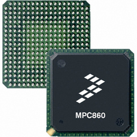
MC68MH360ZP33L Freescale Semiconductor, MC68MH360ZP33L Datasheet - Page 283

MC68MH360ZP33L
Manufacturer Part Number
MC68MH360ZP33L
Description
IC MPU 32BIT QUICC 357-PBGA
Manufacturer
Freescale Semiconductor
Specifications of MC68MH360ZP33L
Processor Type
M683xx 32-Bit
Speed
33MHz
Voltage
5V
Mounting Type
Surface Mount
Package / Case
357-PBGA
Lead Free Status / RoHS Status
Contains lead / RoHS non-compliant
Features
-
Available stocks
Company
Part Number
Manufacturer
Quantity
Price
Company:
Part Number:
MC68MH360ZP33L
Manufacturer:
FREESCALE
Quantity:
1 831
Company:
Part Number:
MC68MH360ZP33L
Manufacturer:
MOTOLOLA
Quantity:
672
Company:
Part Number:
MC68MH360ZP33L
Manufacturer:
Freescale Semiconductor
Quantity:
10 000
Part Number:
MC68MH360ZP33L
Manufacturer:
FREESCALE
Quantity:
20 000
Company:
Part Number:
MC68MH360ZP33LR2
Manufacturer:
Freescale Semiconductor
Quantity:
10 000
- Current page: 283 of 962
- Download datasheet (5Mb)
6.9.3.8 SOFTWARE SERVICE REGISTER (SWSR). The SWSR is the location to which
the SWT servicing sequence is written. To prevent an SWT timeout, the user should write a
$55 followed by a $AA to this register. The SWT can be disabled by clearing the SWE bit in
the SYPCR. The SWSR can be written at any time, but returns all zeros when read.
6.9.3.9 CLKO CONTROL REGISTER (CLKOCR). The CLKOCR controls the operation of
the CLKO2-1 pins. CLKOWP bit in CLKOCR is used as a protect mechanism to prevent
erroneous writing. CLKOCR can be read or written only in supervisor mode.
CLKOWP—CLKOCR Write Protect
Bits 6 -4—Reserved
COM2—Clock Output 2 Mode
COM1—Clock Output 1 Mode
MOTOROLA
This bit protects accidental writing into the CLKOCR. After reset, this bit defaults to zero
to enable writing. Setting this bit prevents further writing (excluding the first write that sets
this bit).
The COM2 bits control the output buffer strength of the CLKO2 pin. When both bits are
set, the CLKO2 pin is held in the high (1) state. These bits can be dynamically changed
without generating spikes on the CLKO2 pin. If the CLKO2 pin is not connected to external
circuits, set both bits (disabling the clock output) to minimize noise and power dissipation.
The COM2 bits are set to ones at system reset, unless MODCK = 01, in which case they
are cleared. This causes CLKO2 to be disabled at system reset, unless MODCK = 01.
(This causes CLKO2 to default to a quiet state, unless it is needed in an MC68040 com-
panion mode system.)
The COM1 bits control the output buffer strength of the CLKO1 pin. When both bits are
set, the CLKO1 pin is held in the high (1) state. These bits can be dynamically changed
00 = Clock Out Enabled, Full-Strength Output Buffer
01 = Clock Out Enabled, 2/3-Strength Output Buffer
10 = Clock Out Enabled, 1/3-Strength Output Buffer
11 = Clock Out Disabled (Driving 1)
If the PIT is enabled with the PTP bit set, then the first interrupt
can be up to 512 clocks early.
CLKOWP
RESET:
7
0
SWSR7
Freescale Semiconductor, Inc.
7
For More Information On This Product,
—
6
0
SWSR6
6
MC68360 USER’S MANUAL
Go to: www.freescale.com
SWSR5
—
5
0
5
SWSR4
—
4
0
4
NOTE
SWSR3
0/1
3
3
COM2
SWSR2
2
0/1
2
SUPERVISOR ONLY
SWSR1
System Integration Module (SIM60)
1
0/1
1
COM1
SWSR0
0
0/1
0
6-39
Related parts for MC68MH360ZP33L
Image
Part Number
Description
Manufacturer
Datasheet
Request
R
Part Number:
Description:
Manufacturer:
Freescale Semiconductor, Inc
Datasheet:
Part Number:
Description:
Manufacturer:
Freescale Semiconductor, Inc
Datasheet:
Part Number:
Description:
Manufacturer:
Freescale Semiconductor, Inc
Datasheet:
Part Number:
Description:
Manufacturer:
Freescale Semiconductor, Inc
Datasheet:
Part Number:
Description:
Manufacturer:
Freescale Semiconductor, Inc
Datasheet:
Part Number:
Description:
Manufacturer:
Freescale Semiconductor, Inc
Datasheet:
Part Number:
Description:
Manufacturer:
Freescale Semiconductor, Inc
Datasheet:
Part Number:
Description:
Manufacturer:
Freescale Semiconductor, Inc
Datasheet:
Part Number:
Description:
Manufacturer:
Freescale Semiconductor, Inc
Datasheet:
Part Number:
Description:
Manufacturer:
Freescale Semiconductor, Inc
Datasheet:
Part Number:
Description:
Manufacturer:
Freescale Semiconductor, Inc
Datasheet:
Part Number:
Description:
Manufacturer:
Freescale Semiconductor, Inc
Datasheet:
Part Number:
Description:
Manufacturer:
Freescale Semiconductor, Inc
Datasheet:
Part Number:
Description:
Manufacturer:
Freescale Semiconductor, Inc
Datasheet:
Part Number:
Description:
Manufacturer:
Freescale Semiconductor, Inc
Datasheet:


