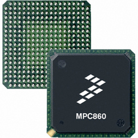
MC68MH360ZP33L Freescale Semiconductor, MC68MH360ZP33L Datasheet - Page 56

MC68MH360ZP33L
Manufacturer Part Number
MC68MH360ZP33L
Description
IC MPU 32BIT QUICC 357-PBGA
Manufacturer
Freescale Semiconductor
Specifications of MC68MH360ZP33L
Processor Type
M683xx 32-Bit
Speed
33MHz
Voltage
5V
Mounting Type
Surface Mount
Package / Case
357-PBGA
Lead Free Status / RoHS Status
Contains lead / RoHS non-compliant
Features
-
Available stocks
Company
Part Number
Manufacturer
Quantity
Price
Company:
Part Number:
MC68MH360ZP33L
Manufacturer:
FREESCALE
Quantity:
1 831
Company:
Part Number:
MC68MH360ZP33L
Manufacturer:
MOTOLOLA
Quantity:
672
Company:
Part Number:
MC68MH360ZP33L
Manufacturer:
Freescale Semiconductor
Quantity:
10 000
Part Number:
MC68MH360ZP33L
Manufacturer:
FREESCALE
Quantity:
20 000
Company:
Part Number:
MC68MH360ZP33LR2
Manufacturer:
Freescale Semiconductor
Quantity:
10 000
- Current page: 56 of 962
- Download datasheet (5Mb)
Signal Descriptions
2.1.7.1 DATA AND SIZE ACKNOWLEDGE (DSACK1–DSACK0). These two active-low
bidirectional signals allow asynchronous data transfers and dynamic data bus sizing
between the QUICC and external devices (see Table 2-3).
2.1.7.2 AUTOVECTOR/INTERRUPT ACKNOWLEDGE (AVEC/IACK5). This pin can be
programmed to be an autovector input or the interrupt acknowledge 5 line output.
AVEC—This signal requests an automatic vector during an interrupt acknowledge cycle.
Refer to Section 6 System Integration Module (SIM60) for more information on the autovec-
tor function. AVEC need not be used if the QUICC supplies the vector internally.
IACK5—The QUICC asserts this pin to indicate the level of an external interrupt during an
interrupt acknowledge cycle at level 5. Peripherals can use the IACKx strobes instead of
monitoring the address bus and function codes to determine that an interrupt acknowledge
cycle is in progress and to obtain the current interrupt level. IACKx lines need not be used
when the vector is generated internally by the QUICC.
2.1.7.3 ADDRESS STROBE (AS). This bidirectional signal is driven by the bus master to
indicate a valid address on the address bus. The function code, size, and read/write signals
are also valid when AS is asserted.
2.1.7.4 DATA STROBE (DS). During a read cycle, this input/output signal is driven by the
bus master to indicate that an external device should place valid data on the data bus. Dur-
ing a write cycle, the data strobe indicates that valid data is on the data bus.
2.1.7.5 TRANSFER SIZE (SIZ1, SIZ0). These bidirectional signals are driven by the bus
master to indicate the number of operand bytes remaining to be transferred in the current
bus cycle (see Table 2-4).
2.1.7.6 READ/WRITE (R/W). This active-high bidirectional signal is driven by the bus mas-
ter to indicate the direction of data transfer on the bus. A logic one indicates a read from a
slave device; a logic zero indicates a write to a slave device.
2-8
0 (Asserted)
0 (Asserted)
1 (Negated)
1 (Negated)
DSACK1
Freescale Semiconductor, Inc.
For More Information On This Product,
0 (Asserted)
0 (Asserted)
1 (Negated)
1 (Negated)
Table 2-3. DSACKx Encoding
DSACK0
SIZ1
Table 2-4. SIZx Encoding
0
1
1
0
MC68360 USER’S MANUAL
Go to: www.freescale.com
Insert wait states in current bus cycle.
Complete cycle—data bus port size is 8 bits.
Complete cycle—data bus port size is 16 bits.
Complete cycle—data bus port size is 32 bits.
SIZ0
1
0
1
0
Byte
Word
3 Bytes
Long Word
Transfer Size
Result
MOTOROLA
Related parts for MC68MH360ZP33L
Image
Part Number
Description
Manufacturer
Datasheet
Request
R
Part Number:
Description:
Manufacturer:
Freescale Semiconductor, Inc
Datasheet:
Part Number:
Description:
Manufacturer:
Freescale Semiconductor, Inc
Datasheet:
Part Number:
Description:
Manufacturer:
Freescale Semiconductor, Inc
Datasheet:
Part Number:
Description:
Manufacturer:
Freescale Semiconductor, Inc
Datasheet:
Part Number:
Description:
Manufacturer:
Freescale Semiconductor, Inc
Datasheet:
Part Number:
Description:
Manufacturer:
Freescale Semiconductor, Inc
Datasheet:
Part Number:
Description:
Manufacturer:
Freescale Semiconductor, Inc
Datasheet:
Part Number:
Description:
Manufacturer:
Freescale Semiconductor, Inc
Datasheet:
Part Number:
Description:
Manufacturer:
Freescale Semiconductor, Inc
Datasheet:
Part Number:
Description:
Manufacturer:
Freescale Semiconductor, Inc
Datasheet:
Part Number:
Description:
Manufacturer:
Freescale Semiconductor, Inc
Datasheet:
Part Number:
Description:
Manufacturer:
Freescale Semiconductor, Inc
Datasheet:
Part Number:
Description:
Manufacturer:
Freescale Semiconductor, Inc
Datasheet:
Part Number:
Description:
Manufacturer:
Freescale Semiconductor, Inc
Datasheet:
Part Number:
Description:
Manufacturer:
Freescale Semiconductor, Inc
Datasheet:


