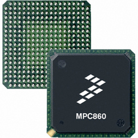
MC68MH360ZP33L Freescale Semiconductor, MC68MH360ZP33L Datasheet - Page 366

MC68MH360ZP33L
Manufacturer Part Number
MC68MH360ZP33L
Description
IC MPU 32BIT QUICC 357-PBGA
Manufacturer
Freescale Semiconductor
Specifications of MC68MH360ZP33L
Processor Type
M683xx 32-Bit
Speed
33MHz
Voltage
5V
Mounting Type
Surface Mount
Package / Case
357-PBGA
Lead Free Status / RoHS Status
Contains lead / RoHS non-compliant
Features
-
Available stocks
Company
Part Number
Manufacturer
Quantity
Price
Company:
Part Number:
MC68MH360ZP33L
Manufacturer:
FREESCALE
Quantity:
1 831
Company:
Part Number:
MC68MH360ZP33L
Manufacturer:
MOTOLOLA
Quantity:
672
Company:
Part Number:
MC68MH360ZP33L
Manufacturer:
Freescale Semiconductor
Quantity:
10 000
Part Number:
MC68MH360ZP33L
Manufacturer:
FREESCALE
Quantity:
20 000
Company:
Part Number:
MC68MH360ZP33LR2
Manufacturer:
Freescale Semiconductor
Quantity:
10 000
- Current page: 366 of 962
- Download datasheet (5Mb)
IDMA Channels
7.6.4.4.4 External Cycle Steal. For external devices that generate a pulsed signal for each
operand to be transferred, the external cycle steal mode should be used. In external cycle
steal mode, the IDMA moves one operand for each falling edge of the DREQx input (see
Figure 7-11). In this mode, DREQx is sampled at each falling edge of the clock to determine
when a valid request is asserted by the device. When the IDMA detects a falling edge on
DREQx, a request becomes pending and remains pending until it is serviced by the IDMA.
Further falling edges on DREQx are ignored until the request begins to be serviced. The ser-
vicing of the request results in one operand being transferred. The operand will be trans-
ferred in back-to-back read and write cycles as long as no other higher priority bus master
or interrupt occurs between the bus cycles.
Each time the IDMA issues a bus cycle to either read or write the device, the IDMA will out-
put the DACKx signal. The device is either the source or destination of the transfers, as
determined by the ECO bit in the CMR. The DACKx timing is similar to the timing of the AS
7-42
ECO = 1; PERIPHERAL IS READ.
NOTES:
(OUTPUT)
(OUTPUT)
(OUTPUT)
ECO = 0; PERIPHERAL IS WRITTEN.
DSACKx
(INPUT)
(INPUT)
3. The sample point for "ANOTHER REQUEST" determines that another IDMA transfer will occur following the current
DREQx
DREQx
DACKx
CLKO1
DACKx
2. This example assumes SRM = 1 in the CMR. If SRM = 0, DREQx would have to be asserted one clock earlier and
1. This example assumes dual address mode. In single address mode, the DREQx sample points would occur in
(I/O)
remain asserted for one clock longer than what is shown to allow it to be internally synchronized by the IDMA
before it is used. Alternatively, the user could assert DREQx as shown and keep DREQx asserted for one
additional clock in the SRM = 0 case, if a wait state were included (between S3 and S4) in all cycles shown above.
IDMA operand transfer. During that time, if the IDMA remains the highest priority bus master of the IMB, the trans-
fers will occur back-to-back as shown.
every IDMA cycle.
AS
S0
OTHER CYCLE
CYCLE STEAL
REQUEST
CYCLE STEAL
REQUEST
S2
S4
Freescale Semiconductor, Inc.
S0
For More Information On This Product,
ANOTHER
REQUEST
Figure 7-11. External Cycle Steal
IDMA READ
S2
MC68360 USER’S MANUAL
Go to: www.freescale.com
S4
S0
ANOTHER
REQUEST
IDMA WRITE
S2
S4
S0
IDMA READ
S2
S4
S0
IDMA WRITE
S2
S4
MOTOROLA
Related parts for MC68MH360ZP33L
Image
Part Number
Description
Manufacturer
Datasheet
Request
R
Part Number:
Description:
Manufacturer:
Freescale Semiconductor, Inc
Datasheet:
Part Number:
Description:
Manufacturer:
Freescale Semiconductor, Inc
Datasheet:
Part Number:
Description:
Manufacturer:
Freescale Semiconductor, Inc
Datasheet:
Part Number:
Description:
Manufacturer:
Freescale Semiconductor, Inc
Datasheet:
Part Number:
Description:
Manufacturer:
Freescale Semiconductor, Inc
Datasheet:
Part Number:
Description:
Manufacturer:
Freescale Semiconductor, Inc
Datasheet:
Part Number:
Description:
Manufacturer:
Freescale Semiconductor, Inc
Datasheet:
Part Number:
Description:
Manufacturer:
Freescale Semiconductor, Inc
Datasheet:
Part Number:
Description:
Manufacturer:
Freescale Semiconductor, Inc
Datasheet:
Part Number:
Description:
Manufacturer:
Freescale Semiconductor, Inc
Datasheet:
Part Number:
Description:
Manufacturer:
Freescale Semiconductor, Inc
Datasheet:
Part Number:
Description:
Manufacturer:
Freescale Semiconductor, Inc
Datasheet:
Part Number:
Description:
Manufacturer:
Freescale Semiconductor, Inc
Datasheet:
Part Number:
Description:
Manufacturer:
Freescale Semiconductor, Inc
Datasheet:
Part Number:
Description:
Manufacturer:
Freescale Semiconductor, Inc
Datasheet:


