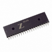
Z85C3010PSG Zilog, Z85C3010PSG Datasheet - Page 29

Z85C3010PSG
Manufacturer Part Number
Z85C3010PSG
Description
IC 10MHZ Z8500 CMOS SCC 40-DIP
Manufacturer
Zilog
Series
SCCr
Specifications of Z85C3010PSG
Processor Type
Z80
Features
Error Detection and Multiprotocol Support
Speed
10MHz
Voltage
5V
Mounting Type
Through Hole
Package / Case
40-DIP (0.620", 15.75mm)
Cpu Speed
8MHz
Digital Ic Case Style
DIP
No. Of Pins
40
Supply Voltage Range
5V
Operating Temperature Range
0°C To +70°C
Svhc
No SVHC (18-Jun-2010)
Base Number
85
Rohs Compliant
Yes
Clock Frequency
10MHz
Lead Free Status / RoHS Status
Lead free / RoHS Compliant
Other names
269-3934
Z85C3010PSG
Z85C3010PSG
Available stocks
Company
Part Number
Manufacturer
Quantity
Price
Company:
Part Number:
Z85C3010PSG
Manufacturer:
Zilog
Quantity:
135
Company:
Part Number:
Z85C3010PSG
Manufacturer:
Zilog
Quantity:
326
- Current page: 29 of 317
- Download datasheet (4Mb)
SCC™/ESCC™ User’s Manual
Interfacing the SCC/ESCC
2.3 Z85X30 INTERFACE TIMING
Two control signals, /RD and /WR, are used by the
Z85X30 to time bus transactions. In addition, four other
control signals, /CE, D//C, A//B and /INTACK, are used to
control the type of bus transaction that occurs. A bus trans-
action starts when the addresses on D//C and A//B are as-
serted before /RD or /WR fall (AC Spec #6 and #8). The
coincidence of /CE and /RD or /CE and /WR latches the
state of D//C and A//B and starts the internal operation.
The /INTACK signal must have been previously sampled
High by a rising edge of PCLK for a read or write cycle to
occur. In addition to sampling /INTACK, PCLK is used by
the interrupt section to set the IP bits.
The Z85X30 generates internal control signals in response
to a register access. Since /RD and /WR have no phase re-
lationship with PCLK, the circuitry generating these inter-
nal control signals provides time for metastable conditions
to disappear. This results in a recovery time related to
PCLK.
2-10
A//B, D//C
/INTACK
D7-D0
/CE
/RD
Figure 2-5. Z85X30 Read Cycle Timing
Address Valid
This recovery time applies only between transactions in-
volving the Z85X30, and any intervening transactions are
ignored. This recovery time is four PCLK cycles (AC Spec
#49), measured from the falling edge of /RD or /WR in the
case of a read or write of any register.
2.3.1 Z85X30 Read Cycle Timing
The read cycle timing for the Z85X30 is shown in
Figure 2-5. The address on A//B and D//C is latched by the
coincidence of /RD and /CE active. /CE must remain Low
and /INTACK must remain High throughout the cycle. The
Z85X30 bus drivers are enabled while /CE and /RD are
both Low. A read with D//C High does not disturb the state
of the pointers and a read cycle with D//C Low resets the
pointers to zero after the internal operation is complete
.
Data Valid
UM010901-0601
Related parts for Z85C3010PSG
Image
Part Number
Description
Manufacturer
Datasheet
Request
R

Part Number:
Description:
Manufacturer:
Zilog, Inc.
Datasheet:

Part Number:
Description:
Cmos Scc Serial Communications Controller
Manufacturer:
ZiLOG Semiconductor
Datasheet:

Part Number:
Description:
Communication Controllers, ZILOG INTELLIGENT PERIPHERAL CONTROLLER (ZIP)
Manufacturer:
Zilog, Inc.
Datasheet:

Part Number:
Description:
KIT DEV FOR Z8 ENCORE 16K TO 64K
Manufacturer:
Zilog
Datasheet:

Part Number:
Description:
KIT DEV Z8 ENCORE XP 28-PIN
Manufacturer:
Zilog
Datasheet:

Part Number:
Description:
DEV KIT FOR Z8 ENCORE 8K/4K
Manufacturer:
Zilog
Datasheet:

Part Number:
Description:
KIT DEV Z8 ENCORE XP 28-PIN
Manufacturer:
Zilog
Datasheet:

Part Number:
Description:
DEV KIT FOR Z8 ENCORE 4K TO 8K
Manufacturer:
Zilog
Datasheet:

Part Number:
Description:
CMOS Z8 microcontroller. ROM 16 Kbytes, RAM 256 bytes, speed 16 MHz, 32 lines I/O, 3.0V to 5.5V
Manufacturer:
Zilog, Inc.
Datasheet:

Part Number:
Description:
Low-cost microcontroller. 512 bytes ROM, 61 bytes RAM, 8 MHz
Manufacturer:
Zilog, Inc.
Datasheet:

Part Number:
Description:
Z8 4K OTP Microcontroller
Manufacturer:
Zilog, Inc.
Datasheet:

Part Number:
Description:
CMOS SUPER8 ROMLESS MCU
Manufacturer:
Zilog, Inc.
Datasheet:

Part Number:
Description:
SL1866 CMOSZ8 OTP Microcontroller
Manufacturer:
Zilog, Inc.
Datasheet:


