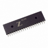
Z85C3010PSG Zilog, Z85C3010PSG Datasheet - Page 125

Z85C3010PSG
Manufacturer Part Number
Z85C3010PSG
Description
IC 10MHZ Z8500 CMOS SCC 40-DIP
Manufacturer
Zilog
Series
SCCr
Specifications of Z85C3010PSG
Processor Type
Z80
Features
Error Detection and Multiprotocol Support
Speed
10MHz
Voltage
5V
Mounting Type
Through Hole
Package / Case
40-DIP (0.620", 15.75mm)
Cpu Speed
8MHz
Digital Ic Case Style
DIP
No. Of Pins
40
Supply Voltage Range
5V
Operating Temperature Range
0°C To +70°C
Svhc
No SVHC (18-Jun-2010)
Base Number
85
Rohs Compliant
Yes
Clock Frequency
10MHz
Lead Free Status / RoHS Status
Lead free / RoHS Compliant
Other names
269-3934
Z85C3010PSG
Z85C3010PSG
Available stocks
Company
Part Number
Manufacturer
Quantity
Price
Company:
Part Number:
Z85C3010PSG
Manufacturer:
Zilog
Quantity:
135
Company:
Part Number:
Z85C3010PSG
Manufacturer:
Zilog
Quantity:
326
- Current page: 125 of 317
- Download datasheet (4Mb)
SCC™/ESCC™ User’s Manual
Register Descriptions
5.1 INTRODUCTION (Continued)
Bits 4 and 3: Transmit Clock select bits 1 and 0.
These bits determine the source of the transmit clock as
shown in Table 5-9. They do not interfere with any of the
modes of operation of the SCC, but simply control a multi-
plexer just before the internal transmit clock input. The
DPLL output that is used to feed the transmitter in FM
modes lags by 90 degrees the output of the DPLL used by
the receiver. This makes the received and transmitted bit
cells occur simultaneously, neglecting delays. A hardware
reset selects the /TRxC pin as the source of the transmit
clocks.
Bit 2: TRxC Pin I/O control bit
This bit determines the direction of the /TRxC pin. If this bit
is set to 1, the /TRxC pin is an output and carries the signal
selected by D1 and D0 of this register. However, if either
the receive or the transmit clock is programmed to come
from the /TRxC pin, /TRxC is an input, regardless of the
state of this bit. The /TRxC pin is also an input if this bit is
set to 0. A hardware reset forces this bit to 0.
Bits 1 and 0: /TRxC Output Source select bits 1 and 0
These bits determine the signal to be echoed out of the
SCC via the /TRxC pin as given in Table 5-10. No signal is
produced if /TRxC has been programmed as the source of
either the receive or the transmit clock. If /TRxC O/I (bit 2)
is set to 0, these bits are ignored.
If the XTAL oscillator output is programmed to be echoed,
and the XTAL oscillator is not enabled, the /TRxC pin goes
High. The DPLL signal that is echoed is the DPLL signal
5-18
Bit 6
Bit 4
0
0
1
1
0
0
1
1
Table 5-8. Receive Clock Source
Table 5-9. Transmit Clock Source
Bit 5
Bit 3
0
1
0
1
0
1
0
1
Receive Clock
/RTxC Pin
/TRxC Pin
BR Output
DPLL Output
Transmit Clock
/RTxC Pin
/TRxC Pin
BR Output
DPLL Output
used by the receiver. Hardware reset selects the XTAL os-
cillator as the output source.
5.2.15 Write Register 12 (Lower Byte of Baud
Rate Generator Time Constant)
WR12 contains the lower byte of the time constant for the
baud rate generator. The time constant can be changed at
any time, but the new value does not take effect until the
next time the time constant is loaded into the down
counter. No attempt is made to synchronize the loading of
the time constant into WR12 and WR13 with the clock driv-
ing the down counter. For this reason, it is advisable to dis-
able the baud rate generator while the new time constant
is loaded into WR12 and WR13. Ordinarily, this is done
anyway to prevent a load of the down counter between the
writing of the upper and lower bytes of the time constant.
The formula for determining the appropriate time constant
for a given baud is shown below, with the desired rate in
bits per second and the BR clock period in seconds. This
formula is derived because the counter decrements from N
down to zero-plus-one-cycle for reloading the time con-
stant. This is then fed to a toggle flip-flop to make the out-
put a square wave. Bit positions for WR12 are shown in
Figure 5-15.
Constant
Write Register 12
D7 D6 D5
Table 5-10. Transmit External Control Selection
Bit 1
Time
0
0
1
1
=
2 x (Desired Rate) x (BR Clock Period)
Figure 5-15. Write Register 12
D4 D3 D2 D1 D0
Bit 0
0
1
0
1
Clock Frequency
TRxC Pin Output
XTAL Oscillator Output
Transmit Clock
BR Output
DPLL Output (receive)
TC0
TC1
TC2
TC3
TC4
TC5
TC6
TC7
UM010901-0601
Lower Byte of
Time Constant
- 2
Related parts for Z85C3010PSG
Image
Part Number
Description
Manufacturer
Datasheet
Request
R

Part Number:
Description:
Manufacturer:
Zilog, Inc.
Datasheet:

Part Number:
Description:
Cmos Scc Serial Communications Controller
Manufacturer:
ZiLOG Semiconductor
Datasheet:

Part Number:
Description:
Communication Controllers, ZILOG INTELLIGENT PERIPHERAL CONTROLLER (ZIP)
Manufacturer:
Zilog, Inc.
Datasheet:

Part Number:
Description:
KIT DEV FOR Z8 ENCORE 16K TO 64K
Manufacturer:
Zilog
Datasheet:

Part Number:
Description:
KIT DEV Z8 ENCORE XP 28-PIN
Manufacturer:
Zilog
Datasheet:

Part Number:
Description:
DEV KIT FOR Z8 ENCORE 8K/4K
Manufacturer:
Zilog
Datasheet:

Part Number:
Description:
KIT DEV Z8 ENCORE XP 28-PIN
Manufacturer:
Zilog
Datasheet:

Part Number:
Description:
DEV KIT FOR Z8 ENCORE 4K TO 8K
Manufacturer:
Zilog
Datasheet:

Part Number:
Description:
CMOS Z8 microcontroller. ROM 16 Kbytes, RAM 256 bytes, speed 16 MHz, 32 lines I/O, 3.0V to 5.5V
Manufacturer:
Zilog, Inc.
Datasheet:

Part Number:
Description:
Low-cost microcontroller. 512 bytes ROM, 61 bytes RAM, 8 MHz
Manufacturer:
Zilog, Inc.
Datasheet:

Part Number:
Description:
Z8 4K OTP Microcontroller
Manufacturer:
Zilog, Inc.
Datasheet:

Part Number:
Description:
CMOS SUPER8 ROMLESS MCU
Manufacturer:
Zilog, Inc.
Datasheet:

Part Number:
Description:
SL1866 CMOSZ8 OTP Microcontroller
Manufacturer:
Zilog, Inc.
Datasheet:


