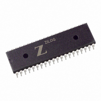
Z85C3010PSG Zilog, Z85C3010PSG Datasheet - Page 204

Z85C3010PSG
Manufacturer Part Number
Z85C3010PSG
Description
IC 10MHZ Z8500 CMOS SCC 40-DIP
Manufacturer
Zilog
Series
SCCr
Specifications of Z85C3010PSG
Processor Type
Z80
Features
Error Detection and Multiprotocol Support
Speed
10MHz
Voltage
5V
Mounting Type
Through Hole
Package / Case
40-DIP (0.620", 15.75mm)
Cpu Speed
8MHz
Digital Ic Case Style
DIP
No. Of Pins
40
Supply Voltage Range
5V
Operating Temperature Range
0°C To +70°C
Svhc
No SVHC (18-Jun-2010)
Base Number
85
Rohs Compliant
Yes
Clock Frequency
10MHz
Lead Free Status / RoHS Status
Lead free / RoHS Compliant
Other names
269-3934
Z85C3010PSG
Z85C3010PSG
Available stocks
Company
Part Number
Manufacturer
Quantity
Price
Company:
Part Number:
Z85C3010PSG
Manufacturer:
Zilog
Quantity:
135
Company:
Part Number:
Z85C3010PSG
Manufacturer:
Zilog
Quantity:
326
- Current page: 204 of 317
- Download datasheet (4Mb)
UM010901-0601
The pin-out of the J5-J10 connectors is fairly consistent,
but of necessity not identical because of differences
Note:
[1] Controlled by the J24 jumper block: must be N/C if (E)SCC channel B transmitter is to be handled by an 80186 DMA channel.
The ground pins are included as signal references with off-
board hardware.
When interconnecting between two connectors among J5-
J10, DO NOT jumper corresponding pins straight across,
as this connects outputs to outputs and inputs to inputs.
Rather, connect at least each pin 1 to the other pin 2, and
Note:
[3] Various conventions have been used to combine synchronous clock inputs and modem control inputs on Apple Macintosh connectors
similar to J4, as described in a later section.
Pin#
1
2
3
4
5
6
7
8
9
10
11
12
Pin #
1
2
3
4
5
6
To use a serial chip controller with the
following on-chip serial interface:
J1A or J1B EIA-RS-232 Console
J2A or J2B EIA-RS-232
RS-422 differential: J3A or J3B EIA-530 or J4 Circular-8 (DIN)
J5: (E)SCC
A pin
TxD
RxD
/RTS
/CTS
/DTR
/DCD
/SYNC
/RTxC
/TRxC
GND
NA
NA
J13-J14
DTE signal
TxD
RxD
/RTS
/CTS
/DTR
/DSR
Table 10. Pin Assignments of Line Driver/Receiver Connectors
Table 9. Pin Assignments of Standard Controller Connectors
J6: (E)SCC
B pin
TxD
RxD
/RTS
/CTS
/DTR or (N/C) [1]
/DCD
/SYNC
/RTxC
/TRxC
GND
NA
NA
Table 8. On-Board Line Driver/Receiver Connectors
J13-J14
DCE signal
RxD
TxD
/CTS
/RTS
/DSR
/DTR
J7,8: ISCC
pin
TxD
RxD
/RTS
/CTS
/DTR
/DCD
/SYNC
/RTxC
/TRxC
GND
NA
NA
J15
DTE signal
TxD
RxD
/RTS
/CTS
/DTR
/DSR
among the various serial controllers:
enough opposing inputs and outputs as needed to make
the communication protocol meaningful.
The pin-out of the 12-pin J13-J15 connectors is similar to
that of J5-J10, but more extensive. To allow for the “DCE”
connectors that were added in revision “B” of the board,
J13 and J14 are 16-pin headers and J15 is a 14-pin one:
J9: IUSC
pin
TxD
RxD
(N/C)
/CTS
(N/C)
/DCD
(SYSCLK)
/RxC
/TxC
GND
/TxREQ
/RxREQ
The Zilog Datacom Family with the 80186 CPU
J15
DCE signal
RxD
TxD
/CTS
/RTS
/DSR
/DTR
Connect the connector(s)
J13
J14
J15
from the previous table to:
J10: MUSC
or USC A pin
TxD
RxD
/RxACK
/CTS
/TxACK
/DCD
(SYSCLK)
/RxC
/TxC
GND
/TxREQ
/RxREQ
Direction/where used
Output to J1-J4
Input from J1-J4
Output to J1-J3
Input from J1-J4 [3]
Output to J1-J4
Input from J1-J4
Application Note
TxD
RxD
/RxACK
/CTS
/TxACK
/DCD
(SYSCLK)
/RxC
/TxC
GND
/TxREQ
/RxREQ
J12: USC
B pin
6-69
8
Related parts for Z85C3010PSG
Image
Part Number
Description
Manufacturer
Datasheet
Request
R

Part Number:
Description:
Manufacturer:
Zilog, Inc.
Datasheet:

Part Number:
Description:
Cmos Scc Serial Communications Controller
Manufacturer:
ZiLOG Semiconductor
Datasheet:

Part Number:
Description:
Communication Controllers, ZILOG INTELLIGENT PERIPHERAL CONTROLLER (ZIP)
Manufacturer:
Zilog, Inc.
Datasheet:

Part Number:
Description:
KIT DEV FOR Z8 ENCORE 16K TO 64K
Manufacturer:
Zilog
Datasheet:

Part Number:
Description:
KIT DEV Z8 ENCORE XP 28-PIN
Manufacturer:
Zilog
Datasheet:

Part Number:
Description:
DEV KIT FOR Z8 ENCORE 8K/4K
Manufacturer:
Zilog
Datasheet:

Part Number:
Description:
KIT DEV Z8 ENCORE XP 28-PIN
Manufacturer:
Zilog
Datasheet:

Part Number:
Description:
DEV KIT FOR Z8 ENCORE 4K TO 8K
Manufacturer:
Zilog
Datasheet:

Part Number:
Description:
CMOS Z8 microcontroller. ROM 16 Kbytes, RAM 256 bytes, speed 16 MHz, 32 lines I/O, 3.0V to 5.5V
Manufacturer:
Zilog, Inc.
Datasheet:

Part Number:
Description:
Low-cost microcontroller. 512 bytes ROM, 61 bytes RAM, 8 MHz
Manufacturer:
Zilog, Inc.
Datasheet:

Part Number:
Description:
Z8 4K OTP Microcontroller
Manufacturer:
Zilog, Inc.
Datasheet:

Part Number:
Description:
CMOS SUPER8 ROMLESS MCU
Manufacturer:
Zilog, Inc.
Datasheet:

Part Number:
Description:
SL1866 CMOSZ8 OTP Microcontroller
Manufacturer:
Zilog, Inc.
Datasheet:


