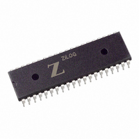
Z85C3010PSG Zilog, Z85C3010PSG Datasheet - Page 174

Z85C3010PSG
Manufacturer Part Number
Z85C3010PSG
Description
IC 10MHZ Z8500 CMOS SCC 40-DIP
Manufacturer
Zilog
Series
SCCr
Specifications of Z85C3010PSG
Processor Type
Z80
Features
Error Detection and Multiprotocol Support
Speed
10MHz
Voltage
5V
Mounting Type
Through Hole
Package / Case
40-DIP (0.620", 15.75mm)
Cpu Speed
8MHz
Digital Ic Case Style
DIP
No. Of Pins
40
Supply Voltage Range
5V
Operating Temperature Range
0°C To +70°C
Svhc
No SVHC (18-Jun-2010)
Base Number
85
Rohs Compliant
Yes
Clock Frequency
10MHz
Lead Free Status / RoHS Status
Lead free / RoHS Compliant
Other names
269-3934
Z85C3010PSG
Z85C3010PSG
Available stocks
Company
Part Number
Manufacturer
Quantity
Price
Company:
Part Number:
Z85C3010PSG
Manufacturer:
Zilog
Quantity:
135
Company:
Part Number:
Z85C3010PSG
Manufacturer:
Zilog
Quantity:
326
- Current page: 174 of 317
- Download datasheet (4Mb)
UM010901-0601
I/O Read Cycle
These tables show that a delay of the falling edge of /RD
satisfies the SCC TsA(RD) timing requirement of 50 ns
min. The Z180 calculated value is 30 ns min for the worst
case. Also, Z180 timing specification tAH (Address Hold
time) is 10 ns min. The SCC timing parameters ThA(RD)
{Address to /RD High Hold} and ThCE(RD) {/CE to /RD
High Hold} are minimum at 0 ns. The rising edge of /RD is
early to guarantee these parameters when considering
address decoders and gate propagation delays.
I/O Write Cycle
Delay the falling edge of /WR to satisfy the SCC TsA(/WR)
timing requirement of 50 ns min. The Z180 calculates 30
SCC
Parameters
TsA(RD)
TdA(DR)
TdRDf(DR)
TwRDI
TsA(WR)
TsDW(WR)
TwWRI
Z180
Parameters
tDRS
Table 8. Parameter Equations Worst Case (Without Delay Signals - No Wait State)
Z180
Equation
tcyc-tAD+tRDD1
3tcyc+tCHW+tcf-tAD-tDRS
2tcyc+tCHW+tcf-tRDD1-tDRS
2tcyc+tCHW+tcf-tDRS+tRDD2
tcyc-tAD+tWRD1
tWDS
tWRP
SCC
Equation
Address
3tcyc+tCHW-tAD-TdA(DR)
RD
2tcyc+tCHW-tRDD1-TdRD(DR)
Table 9. Parameter Equations
ns min worst case. Further, the Z180 timing specifications
tAH (Address Hold time) and tWDH (/WR high to data hold
time) are both 10 ns min. The SCC timing parameters
ThA(WR) {Address to /WR High Hold}, ThCE(WR) {/CE to
/WR High Hold} and TdWR(W) {Write data to /WR High
hold} are a minimum of 0 ns. The rising edge of /WR is
early to guarantee these parameter requirements.
This circuit depicts logic for the I/O interface and the
Interrupt Acknowledge Interface for 10 MHz clock of
operation. Figure 13 is the I/O read/write timing chart
(discussions of timing considerations on the Interrupt
Acknowledge cycle and the circuit using EPLD occur
later).
The Z180™ Interfaced with the SCC at MHZ
245 min
160 min
185 min
210 min
241 min
184 min
30 min
30 min
15 min
Value
Value
Application Note
Units
Units
ns
ns
ns
ns
ns
ns
ns
ns
ns
6-39
7
Related parts for Z85C3010PSG
Image
Part Number
Description
Manufacturer
Datasheet
Request
R

Part Number:
Description:
Manufacturer:
Zilog, Inc.
Datasheet:

Part Number:
Description:
Cmos Scc Serial Communications Controller
Manufacturer:
ZiLOG Semiconductor
Datasheet:

Part Number:
Description:
Communication Controllers, ZILOG INTELLIGENT PERIPHERAL CONTROLLER (ZIP)
Manufacturer:
Zilog, Inc.
Datasheet:

Part Number:
Description:
KIT DEV FOR Z8 ENCORE 16K TO 64K
Manufacturer:
Zilog
Datasheet:

Part Number:
Description:
KIT DEV Z8 ENCORE XP 28-PIN
Manufacturer:
Zilog
Datasheet:

Part Number:
Description:
DEV KIT FOR Z8 ENCORE 8K/4K
Manufacturer:
Zilog
Datasheet:

Part Number:
Description:
KIT DEV Z8 ENCORE XP 28-PIN
Manufacturer:
Zilog
Datasheet:

Part Number:
Description:
DEV KIT FOR Z8 ENCORE 4K TO 8K
Manufacturer:
Zilog
Datasheet:

Part Number:
Description:
CMOS Z8 microcontroller. ROM 16 Kbytes, RAM 256 bytes, speed 16 MHz, 32 lines I/O, 3.0V to 5.5V
Manufacturer:
Zilog, Inc.
Datasheet:

Part Number:
Description:
Low-cost microcontroller. 512 bytes ROM, 61 bytes RAM, 8 MHz
Manufacturer:
Zilog, Inc.
Datasheet:

Part Number:
Description:
Z8 4K OTP Microcontroller
Manufacturer:
Zilog, Inc.
Datasheet:

Part Number:
Description:
CMOS SUPER8 ROMLESS MCU
Manufacturer:
Zilog, Inc.
Datasheet:

Part Number:
Description:
SL1866 CMOSZ8 OTP Microcontroller
Manufacturer:
Zilog, Inc.
Datasheet:


