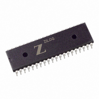
Z85C3010PSG Zilog, Z85C3010PSG Datasheet - Page 196

Z85C3010PSG
Manufacturer Part Number
Z85C3010PSG
Description
IC 10MHZ Z8500 CMOS SCC 40-DIP
Manufacturer
Zilog
Series
SCCr
Specifications of Z85C3010PSG
Processor Type
Z80
Features
Error Detection and Multiprotocol Support
Speed
10MHz
Voltage
5V
Mounting Type
Through Hole
Package / Case
40-DIP (0.620", 15.75mm)
Cpu Speed
8MHz
Digital Ic Case Style
DIP
No. Of Pins
40
Supply Voltage Range
5V
Operating Temperature Range
0°C To +70°C
Svhc
No SVHC (18-Jun-2010)
Base Number
85
Rohs Compliant
Yes
Clock Frequency
10MHz
Lead Free Status / RoHS Status
Lead free / RoHS Compliant
Other names
269-3934
Z85C3010PSG
Z85C3010PSG
Available stocks
Company
Part Number
Manufacturer
Quantity
Price
Company:
Part Number:
Z85C3010PSG
Manufacturer:
Zilog
Quantity:
135
Company:
Part Number:
Z85C3010PSG
Manufacturer:
Zilog
Quantity:
326
- Current page: 196 of 317
- Download datasheet (4Mb)
UM010901-0601
Push buttons are provided for Reset and Non-Maskable
Interrupt (NMI). A means to generate an NMI, in response
to a Start bit received from the user’s PC or terminal, is
also provided. The first transmitted Start bit on the RS-232.
Console connector J1, after a Reset, also produces an
NMI; this feature can be used to find which serial controller
channel is connected to the Console connector.
Address Map
EPROM is located at the highest addresses, and its size is
programmable in the 80186 for the /UCS output. The
EPROM
Two 28-pin EPROM sockets are provided; both must be
populated in order to handle the 80186’s 16-bit instruction
fetches. Jumper header J18 allows the sockets to be
compatible with 2764s, 27128s, 27256s, or 27512s; it is
jumpered at the factory to match the EPROMs provided.
For 27512s only, jumper J18-J2 to J18-J3 and leave J18-
J1 open. For 2764s, 27128s, or 27256s, jumper J18-J2 to
J18-J1 and leave J18-J3 open.
Note: J18 connects pin 1 of both sockets to either A16 or
Vcc. This is done because for 2764s, 27128s, and 27256s,
pin 1 is Vpp which may require a high voltage and/or draw
more current than a normal logic input. For 2764s and
27128s, a similar jumper might be provided in some
designs for pin 27 (/PGM). As long as the address for /UCS
is programmed as described in the next paragraph, A15
(which is connected to pin 27) is High whenever /UCS is
Low, so that 2764s and 27128s operate correctly.
The first code executed after Reset should program the
80186’s Chip Select Control Registers to set up the
address ranges for which outputs like /UCS and /PCS6-
/PCS0 are asserted. In particular, the UMCS register
(address A0H within the 80186’s Peripheral Control Block)
RAM
(E)SCC
ISCC
(M)USC
IUSC
ISCC-IUSC-(M)USC Reset
27512 EPROM
Table 3. Suggested Address Map
addresses of the datacom controllers are programmed in
the 80186 for the /PCS6-/PCS0 outputs, as a block of
128x7=896 bytes starting at a 1 Kbyte boundary. The
block can be in I/O space or in a part of memory space that
is not used for SRAM or EPROM. The starting 1 Kbyte
boundary is called (PBA) in the following sections.
RAM extends upward from address 0.
Using 128K x 8 SRAMs and 64K x 8 EPROMs, the
address map might be as shown in Table 3.
must be programmed to correspond to the size of
EPROMs used (Table 4).
EPROM
Type
The three LSBs of the above UMCS values are all 100,
which signifies no external Ready/WAIT is used and no
wait states are required. If the EPROMs are not fast
enough for no-wait-state operation, making the three LSBs
101, 110, or 111 extends EPROM cycles by 1, 2, or 3 wait
states, respectively.
00000-BFFFF
D8000, 2, 4, 6 or D8000-D803E (even addrs only)
D8080-D80FE (even addrs only)
D8100-D81FF
D8200-D837F
DB000-DB7FF (if enabled)
E0000-FFFFF
The Zilog Datacom Family with the 80186 CPU
Table 4. EPROM Address Ranges
UMCS Value
27128
27256
27512
2764
EPROM
FC3C
E03C
F83C
F03C
Application Note
Address
Range
FC000-FFFFF
F8000-FFFFF
F0000-FFFFF
E0000-FFFFF
6-61
8
Related parts for Z85C3010PSG
Image
Part Number
Description
Manufacturer
Datasheet
Request
R

Part Number:
Description:
Manufacturer:
Zilog, Inc.
Datasheet:

Part Number:
Description:
Cmos Scc Serial Communications Controller
Manufacturer:
ZiLOG Semiconductor
Datasheet:

Part Number:
Description:
Communication Controllers, ZILOG INTELLIGENT PERIPHERAL CONTROLLER (ZIP)
Manufacturer:
Zilog, Inc.
Datasheet:

Part Number:
Description:
KIT DEV FOR Z8 ENCORE 16K TO 64K
Manufacturer:
Zilog
Datasheet:

Part Number:
Description:
KIT DEV Z8 ENCORE XP 28-PIN
Manufacturer:
Zilog
Datasheet:

Part Number:
Description:
DEV KIT FOR Z8 ENCORE 8K/4K
Manufacturer:
Zilog
Datasheet:

Part Number:
Description:
KIT DEV Z8 ENCORE XP 28-PIN
Manufacturer:
Zilog
Datasheet:

Part Number:
Description:
DEV KIT FOR Z8 ENCORE 4K TO 8K
Manufacturer:
Zilog
Datasheet:

Part Number:
Description:
CMOS Z8 microcontroller. ROM 16 Kbytes, RAM 256 bytes, speed 16 MHz, 32 lines I/O, 3.0V to 5.5V
Manufacturer:
Zilog, Inc.
Datasheet:

Part Number:
Description:
Low-cost microcontroller. 512 bytes ROM, 61 bytes RAM, 8 MHz
Manufacturer:
Zilog, Inc.
Datasheet:

Part Number:
Description:
Z8 4K OTP Microcontroller
Manufacturer:
Zilog, Inc.
Datasheet:

Part Number:
Description:
CMOS SUPER8 ROMLESS MCU
Manufacturer:
Zilog, Inc.
Datasheet:

Part Number:
Description:
SL1866 CMOSZ8 OTP Microcontroller
Manufacturer:
Zilog, Inc.
Datasheet:


