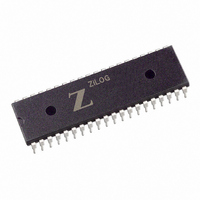
Z85C3010PSG Zilog, Z85C3010PSG Datasheet - Page 163

Z85C3010PSG
Manufacturer Part Number
Z85C3010PSG
Description
IC 10MHZ Z8500 CMOS SCC 40-DIP
Manufacturer
Zilog
Series
SCCr
Specifications of Z85C3010PSG
Processor Type
Z80
Features
Error Detection and Multiprotocol Support
Speed
10MHz
Voltage
5V
Mounting Type
Through Hole
Package / Case
40-DIP (0.620", 15.75mm)
Cpu Speed
8MHz
Digital Ic Case Style
DIP
No. Of Pins
40
Supply Voltage Range
5V
Operating Temperature Range
0°C To +70°C
Svhc
No SVHC (18-Jun-2010)
Base Number
85
Rohs Compliant
Yes
Clock Frequency
10MHz
Lead Free Status / RoHS Status
Lead free / RoHS Compliant
Other names
269-3934
Z85C3010PSG
Z85C3010PSG
Available stocks
Company
Part Number
Manufacturer
Quantity
Price
Company:
Part Number:
Z85C3010PSG
Manufacturer:
Zilog
Quantity:
135
Company:
Part Number:
Z85C3010PSG
Manufacturer:
Zilog
Quantity:
326
- Current page: 163 of 317
- Download datasheet (4Mb)
Application Note
The Z180™ Interfaced with the SCC at MHZ
EPROM INTERFACE
During an Opcode fetch cycle, data sampling of the bus is
on the rising PHI clock edge of T3 and on the falling edge
of T3 during a memory read cycle. Opcode fetch cycle data
sample timing is half a clock cycle earlier. Table 2 shows
how a memory read cycles’ timing requirements are easier
than an opcode fetch cycle by half a PHI cycle time. If the
Note: * w is the number of wait states.
The propagation delay for the decoded address and gates
in the previous calculation is zero. Hence, on the real
design, subtracting another 20-30 ns to pay for
propagation delays, is possible. The 27C256 provides the
EPROM for this board. Typical timing parameters for the
27C256 are in Table 3.
Note: Table 3 shows “Access Time” as applying /E to data valid.
“/OE active to data valid” is shorter than “address access time”.
Hence, the interface logic for the EPROM is: Realize a 170 ns or
faster EPROM access time by adding one wait state (using the
on-chip wait state generator of the Z180). A 200 ns requirement
uses two wait states for memory access.
SRAM Interface
Table 4 has timing parameters for 256K bit SRAM for this
design.)
6-28
Table 3. EPROM (27C256) Key Timing Parameters
Parameters
Address Valid to Data Valid (Opcode Fetch)
Address Valid to Data Valid (Memory Read
/MREQ Active to Data Valid (Opcode Fetch)
/MREQ Active to Data Valid (Memory Read)
/RD Active to Data Valid (Opcode Fetch)
/RD Active to Data Valid (Memory Read)
Memory Write Cycle /WR Pulse Width
Parameter
Addr Access Time
/E to Data Valid
/OE to Data Valid
(Values May Vary Depending On Mfg.)
Table 2. Parameter Equations (10 MHz) Opcode Fetch/Memory Read/Write Cycle
170 ns 200 ns 250 ns
Max
170
170
75
Access Time
Max
200
200
75
Max
250
250
100
Z180 Equation
2(1+w)tcyc-tAD-tDRS
2(1+w)tcyc+tCHW+tcf-tAD-tDRS
(2+w)tcyc-tMED1-tDRS
(1+w)tcyc+tCLW-tRRD1-tDRS
(2+w)tcyc-tRRD1-tDRS
tWRP+w*tcyc
(1+w)tcyc+tCLW-tMED1-tDRS
timing requirements for an Opcode fetch cycle meet
specifications, the design satisfies the timing requirements
for a memory read cycle.
Table 2 has some equations for an opcode fetch, memory
read/write cycle.
SRAM Read Cycle. An SRAM read cycle shares the
same considerations as an EPROM interface.
Like EPROM, SRAMs’ “access time” applies /G to data
valid, and “/E active to data valid” is shorter than “access
time.” This design allows the use of a 150 ns access time
SRAM by adding one wait state (using the on-chip wait
state generator of the Z180). The circuit is common to the
EPROM memory read cycle.
No wait states are necessary if there is a 85 ns, or faster,
access time by using SRAMs. Since the Z180 has on-chip
MMU with 85 ns or faster SRAM just copy the contents of
EPROM (application program starts at logical address
0000h) into SRAM after power on. Set up the MMU to
SRAM area to override the EPROM area and stop
Parameter
Read Cycle:
/E to Data Valid
/G to Data Valid
Write Cycle:
Write Cycle Time
Addr Valid to End of Write
Chip Select to End of Write
Data Select to End of Write
Write Pulse Width
Addr Setup Time
Table 4. 256K SRAM Key Timing parameters
(Values May Vary Depending On Mfg.)
105+100w min
155+100w min
105+100w min
55+100w min
105+100w min
110+100w min
55+100w min
85 ns 100 ns 150 ns
Min
85
45
85
75
75
40
60
0
Value
Access Time
UM010901-0601
Min
100
100
40
80
80
40
60
0
Units
ns
Min
150
150
100
100
ns
ns
ns
ns
ns
ns
60
60
90
0
Related parts for Z85C3010PSG
Image
Part Number
Description
Manufacturer
Datasheet
Request
R

Part Number:
Description:
Manufacturer:
Zilog, Inc.
Datasheet:

Part Number:
Description:
Cmos Scc Serial Communications Controller
Manufacturer:
ZiLOG Semiconductor
Datasheet:

Part Number:
Description:
Communication Controllers, ZILOG INTELLIGENT PERIPHERAL CONTROLLER (ZIP)
Manufacturer:
Zilog, Inc.
Datasheet:

Part Number:
Description:
KIT DEV FOR Z8 ENCORE 16K TO 64K
Manufacturer:
Zilog
Datasheet:

Part Number:
Description:
KIT DEV Z8 ENCORE XP 28-PIN
Manufacturer:
Zilog
Datasheet:

Part Number:
Description:
DEV KIT FOR Z8 ENCORE 8K/4K
Manufacturer:
Zilog
Datasheet:

Part Number:
Description:
KIT DEV Z8 ENCORE XP 28-PIN
Manufacturer:
Zilog
Datasheet:

Part Number:
Description:
DEV KIT FOR Z8 ENCORE 4K TO 8K
Manufacturer:
Zilog
Datasheet:

Part Number:
Description:
CMOS Z8 microcontroller. ROM 16 Kbytes, RAM 256 bytes, speed 16 MHz, 32 lines I/O, 3.0V to 5.5V
Manufacturer:
Zilog, Inc.
Datasheet:

Part Number:
Description:
Low-cost microcontroller. 512 bytes ROM, 61 bytes RAM, 8 MHz
Manufacturer:
Zilog, Inc.
Datasheet:

Part Number:
Description:
Z8 4K OTP Microcontroller
Manufacturer:
Zilog, Inc.
Datasheet:

Part Number:
Description:
CMOS SUPER8 ROMLESS MCU
Manufacturer:
Zilog, Inc.
Datasheet:

Part Number:
Description:
SL1866 CMOSZ8 OTP Microcontroller
Manufacturer:
Zilog, Inc.
Datasheet:


