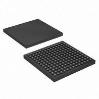
EP4CGX15BF14C8N Altera, EP4CGX15BF14C8N Datasheet - Page 383

EP4CGX15BF14C8N
Manufacturer Part Number
EP4CGX15BF14C8N
Description
IC CYCLONE IV FPGA 15K 169FBGA
Manufacturer
Altera
Series
CYCLONE® IV GXr
Datasheets
1.EP4CGX15BN11C8N.pdf
(44 pages)
2.EP4CGX15BN11C8N.pdf
(14 pages)
3.EP4CGX15BN11C8N.pdf
(478 pages)
4.EP4CGX15BN11C8N.pdf
(10 pages)
Specifications of EP4CGX15BF14C8N
Number Of Logic Elements/cells
14400
Number Of Labs/clbs
900
Total Ram Bits
540000
Number Of I /o
72
Voltage - Supply
1.16 V ~ 1.24 V
Mounting Type
Surface Mount
Operating Temperature
0°C ~ 85°C
Package / Case
169-FBGA
Lead Free Status / RoHS Status
Lead free / RoHS Compliant
Number Of Gates
-
Other names
544-1475
Available stocks
Company
Part Number
Manufacturer
Quantity
Price
Company:
Part Number:
EP4CGX15BF14C8N
Manufacturer:
ALTERA33
Quantity:
276
- EP4CGX15BN11C8N PDF datasheet
- EP4CGX15BN11C8N PDF datasheet #2
- EP4CGX15BN11C8N PDF datasheet #3
- EP4CGX15BN11C8N PDF datasheet #4
- Current page: 383 of 478
- Download datasheet (13Mb)
Chapter 2: Cyclone IV Reset Control and Power Down
Transceiver Reset Sequences
© December 2010 Altera Corporation
PCIe Initialization/Compliance Phase
After the device is powered up, a PCIe-compliant device goes through the compliance
phase during initialization. The rx_digitalreset signal must be deasserted
during this compliance phase to achieve transitions on the pipephydonestatus
signal, as expected by the link layer. The rx_digitalreset signal is deasserted
based on the assertion of the rx_freqlocked signal.
During the initialization/compliance phase, do not use the rx_freqlocked signal to
trigger a deassertion of the rx_digitalreset signal. Instead, perform the following
reset sequence:
1. After power up, assert pll_areset for a minimum period of 1 s (the time
2. After the multipurpose PLL locks, as indicated by the pll_locked signal going
3. Deassert both the rx_analogreset signal (marker 6) and rx_digitalreset
PCIe Normal Phase
For the normal PCIe phase:
1. After completion of the Initialization/Compliance phase, during the normal
2. Wait for the rx_freqlocked signal to go high again. In this phase, the received
3. After the rx_freqlocked signal goes high, wait for at least t
between markers 1 and 2). Keep the tx_digitalreset, rx_analogreset, and
rx_digitalreset signals asserted during this time period. After you deassert
the pll_areset signal, the multipurpose PLL starts locking to the input
reference clock.
high (marker 3), deassert tx_digitalreset. For a receiver operation, after
deassertion of busy signal, wait for two parallel clock cycles to deassert the
rx_analogreset signal. After rx_analogreset is deasserted, the receiver
CDR starts locking to the receiver input reference clock.
signal (marker 7) together, as indicated in
rx_digitalreset, the pipephydonestatus signal transitions from the
transceiver channel to indicate the status to the link layer. Depending on its status,
pipephydonestatus helps with the continuation of the compliance phase. After
successful completion of this phase, the device enters into the normal operation
phase.
operation phase at the Gen1 data rate, when the rx_freqlocked signal is
deasserted (marker 9 in
data is valid (not electrical idle) and the receiver CDR locks to the incoming data.
Proceed with the reset sequence after assertion of the rx_freqlocked signal.
asserting rx_digitalreset (marker 12 in
clock cycles so that the receiver phase compensation FIFO is initialized. For
bonded PCIe Gen 1 mode (×2 and ×4), wait for all the rx_freqlocked signals to
go high, then wait for t
clock cycles.
LTD_Manual
Figure
2–10).
before asserting rx_digitalreset for 2 parallel
Figure
Figure
2–10. After deasserting
2–10) for two parallel receive
Cyclone IV Device Handbook, Volume 2
LTD_Manual
before
2–17
Related parts for EP4CGX15BF14C8N
Image
Part Number
Description
Manufacturer
Datasheet
Request
R

Part Number:
Description:
CYCLONE II STARTER KIT EP2C20N
Manufacturer:
Altera
Datasheet:

Part Number:
Description:
CPLD, EP610 Family, ECMOS Process, 300 Gates, 16 Macro Cells, 16 Reg., 16 User I/Os, 5V Supply, 35 Speed Grade, 24DIP
Manufacturer:
Altera Corporation
Datasheet:

Part Number:
Description:
CPLD, EP610 Family, ECMOS Process, 300 Gates, 16 Macro Cells, 16 Reg., 16 User I/Os, 5V Supply, 15 Speed Grade, 24DIP
Manufacturer:
Altera Corporation
Datasheet:

Part Number:
Description:
Manufacturer:
Altera Corporation
Datasheet:

Part Number:
Description:
CPLD, EP610 Family, ECMOS Process, 300 Gates, 16 Macro Cells, 16 Reg., 16 User I/Os, 5V Supply, 30 Speed Grade, 24DIP
Manufacturer:
Altera Corporation
Datasheet:

Part Number:
Description:
High-performance, low-power erasable programmable logic devices with 8 macrocells, 10ns
Manufacturer:
Altera Corporation
Datasheet:

Part Number:
Description:
High-performance, low-power erasable programmable logic devices with 8 macrocells, 7ns
Manufacturer:
Altera Corporation
Datasheet:

Part Number:
Description:
Classic EPLD
Manufacturer:
Altera Corporation
Datasheet:

Part Number:
Description:
High-performance, low-power erasable programmable logic devices with 8 macrocells, 10ns
Manufacturer:
Altera Corporation
Datasheet:

Part Number:
Description:
Manufacturer:
Altera Corporation
Datasheet:

Part Number:
Description:
Manufacturer:
Altera Corporation
Datasheet:

Part Number:
Description:
Manufacturer:
Altera Corporation
Datasheet:

Part Number:
Description:
CPLD, EP610 Family, ECMOS Process, 300 Gates, 16 Macro Cells, 16 Reg., 16 User I/Os, 5V Supply, 25 Speed Grade, 24DIP
Manufacturer:
Altera Corporation
Datasheet:


