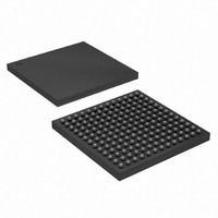
EP4CGX15BF14C8N Altera, EP4CGX15BF14C8N Datasheet - Page 304

EP4CGX15BF14C8N
Manufacturer Part Number
EP4CGX15BF14C8N
Description
IC CYCLONE IV FPGA 15K 169FBGA
Manufacturer
Altera
Series
CYCLONE® IV GXr
Datasheets
1.EP4CGX15BN11C8N.pdf
(44 pages)
2.EP4CGX15BN11C8N.pdf
(14 pages)
3.EP4CGX15BN11C8N.pdf
(478 pages)
4.EP4CGX15BN11C8N.pdf
(10 pages)
Specifications of EP4CGX15BF14C8N
Number Of Logic Elements/cells
14400
Number Of Labs/clbs
900
Total Ram Bits
540000
Number Of I /o
72
Voltage - Supply
1.16 V ~ 1.24 V
Mounting Type
Surface Mount
Operating Temperature
0°C ~ 85°C
Package / Case
169-FBGA
Lead Free Status / RoHS Status
Lead free / RoHS Compliant
Number Of Gates
-
Other names
544-1475
Available stocks
Company
Part Number
Manufacturer
Quantity
Price
Company:
Part Number:
EP4CGX15BF14C8N
Manufacturer:
ALTERA33
Quantity:
276
- EP4CGX15BN11C8N PDF datasheet
- EP4CGX15BN11C8N PDF datasheet #2
- EP4CGX15BN11C8N PDF datasheet #3
- EP4CGX15BN11C8N PDF datasheet #4
- Current page: 304 of 478
- Download datasheet (13Mb)
1–24
Transceiver Clocking Architecture
Input Reference Clocking
Cyclone IV Device Handbook, Volume 2
1
The multipurpose PLLs and general-purpose PLLs located on the left side of the
device generate the clocks required for the transceiver operation. The following
sections describe the Cyclone IV GX transceiver clocking architecture:
■
■
■
When used for transceiver, the left PLLs synthesize the input reference clock to
generate the required clocks for the transceiver channels.
show the sources of input reference clocks for PLLs used in the transceiver operation.
Clock output from PLLs in the FPGA core cannot feed into PLLs used by the
transceiver as input reference clock.
Figure 1–25. PLL Input Reference Clocks in Transceiver Operation for F324 and Smaller Packages
Notes to
(1) The REFCLK0 and REFCLK1 pins are dual-purpose CLK, REFCLK, or DIFFCLK pins that reside in banks 3A and
(2) Using any clock input pins other than the designated REFCLK pins as shown here to drive the MPLLs may have
(Note
“Input Reference Clocking” on page 1–24
“Transceiver Channel Datapath Clocking” on page 1–26
“FPGA Fabric-Transceiver Interface Clocking” on page 1–39
8A respectively.
reduced jitter performance.
1),
Figure
(2)
1–25:
Transceiver
MPLL_2
MPLL_1
GXBL0
Block
REFCLK1
REFCLK0
Chapter 1: Cyclone IV Transceivers Architecture
Figure 1–25
© December 2010 Altera Corporation
Transceiver Clocking Architecture
and
Figure 1–26
Related parts for EP4CGX15BF14C8N
Image
Part Number
Description
Manufacturer
Datasheet
Request
R

Part Number:
Description:
CYCLONE II STARTER KIT EP2C20N
Manufacturer:
Altera
Datasheet:

Part Number:
Description:
CPLD, EP610 Family, ECMOS Process, 300 Gates, 16 Macro Cells, 16 Reg., 16 User I/Os, 5V Supply, 35 Speed Grade, 24DIP
Manufacturer:
Altera Corporation
Datasheet:

Part Number:
Description:
CPLD, EP610 Family, ECMOS Process, 300 Gates, 16 Macro Cells, 16 Reg., 16 User I/Os, 5V Supply, 15 Speed Grade, 24DIP
Manufacturer:
Altera Corporation
Datasheet:

Part Number:
Description:
Manufacturer:
Altera Corporation
Datasheet:

Part Number:
Description:
CPLD, EP610 Family, ECMOS Process, 300 Gates, 16 Macro Cells, 16 Reg., 16 User I/Os, 5V Supply, 30 Speed Grade, 24DIP
Manufacturer:
Altera Corporation
Datasheet:

Part Number:
Description:
High-performance, low-power erasable programmable logic devices with 8 macrocells, 10ns
Manufacturer:
Altera Corporation
Datasheet:

Part Number:
Description:
High-performance, low-power erasable programmable logic devices with 8 macrocells, 7ns
Manufacturer:
Altera Corporation
Datasheet:

Part Number:
Description:
Classic EPLD
Manufacturer:
Altera Corporation
Datasheet:

Part Number:
Description:
High-performance, low-power erasable programmable logic devices with 8 macrocells, 10ns
Manufacturer:
Altera Corporation
Datasheet:

Part Number:
Description:
Manufacturer:
Altera Corporation
Datasheet:

Part Number:
Description:
Manufacturer:
Altera Corporation
Datasheet:

Part Number:
Description:
Manufacturer:
Altera Corporation
Datasheet:

Part Number:
Description:
CPLD, EP610 Family, ECMOS Process, 300 Gates, 16 Macro Cells, 16 Reg., 16 User I/Os, 5V Supply, 25 Speed Grade, 24DIP
Manufacturer:
Altera Corporation
Datasheet:


